概览
描述
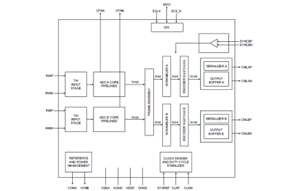
The ADC1453D250 is a dual channel 14-bit analog-to-digital converter (ADC) with JESD204B serial outputs interface optimized for high dynamic performance and low power consumption at sample rates up to 250Msps. Pipelined architecture and output error correction ensure the ADC1453D250 is accurate enough to guarantee zero missing codes over the entire operating range. Supplied from a single 1.8V source, the ADC1453D complies to the JESD204B serial output standard. An integrated serial peripheral interface (SPI) allows easy configuration of the ADC. With excellent dynamic performance from the baseband to input frequencies of 250MHz or more, the ADC1453D250 is ideal for use in undersampled multi-carrier, multi-standard communication system applications.
特性
- Dual channel 14-bit ADC, Sampling rate up to 250Msps
- JESD204B device Subclass 0, Subclass 1, Subclass 2 support
- SYSREF based deterministic and repeatable interface latency
- Multiple device synchronization and harmonic clocking
- 2-lane JESD204B serial output interface up to 5Gbps
- Clock input divider from 1 to 8
- Duty cycle stabilizer
- Flexible Analog input 1V (p-p) to 2V (p-p)
- Offset binary and two's complement and gray output data
- Power-down and sleep modes
- Serial peripheral interface (SPI)
- Single 1.8V supply
- Industrial temperature range
产品对比
应用
- Wireless infrastructure: LTE, TD-LTE, WiMAX, MC-GSM, CDMA, WCDMA, TD-SCDMA
- Microwave backhaul transceivers
- Software defined radio
- Aerospace and defense communications and radar systems
- Medical non-invasive scanners
- Industrial signal analysis instruments
- Scientific particle detectors
- General-purpose high-speed applications
设计和开发
模型
ECAD 模块
点击产品选项表中的产品,查找 SamacSys 中的原理图符号、PCB 足迹和 3D CAD 模型。点击产品选项表中的产品,查找 SamacSys 中的原理图符号、PCB 足迹和 3D CAD 模型。

产品选项
当前筛选条件
