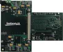
High Speed A/D Converter Evaluation Kits
Renesas offers two options for evaluating high-speed analog-to-digital converter (ADC) products with LVDS and/or LVCMOS outputs. A complete, turnkey evaluation platform...
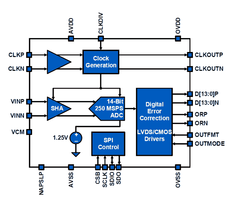
The KAD5514P (KAD5514P-12, KAD5514P-17, KAD5514P-21, KAD5514P-25) is a family of low-power, high performance 14-bit, analog-to-digital converters. The family is designed with the proprietary FemtoCharge™ technology on a standard CMOS process, and supports sampling rates of up to 250MSPS. The KAD5514P is part of a pin-compatible portfolio of 10, 12, and 14-bit ADCs with sample rates ranging from 125MSPS to 500MSPS. A Serial Peripheral Interface (SPI) port allows for extensive configurability and fine control of various parameters such as gain and offset. Digital output data is presented in selectable LVDS or CMOS formats. The KAD5514P is available in 72 Ld and 48 Ld QFN packages with an exposed paddle. The devices operate from a 1. 8V supply, and performance is specified across the full industrial temperature range (-40°C to +85°C).
|
|
|
|
|---|---|---|
| 类型 | 文档标题 | 日期 |
| 数据手册 | PDF 825 KB | |
| 宣传手册 | PDF 5.41 MB 日本語 | |
| 产品变更通告 | PDF 341 KB | |
| 指南 | PDF 1.02 MB | |
| 手册 - 开发工具 | PDF 509 KB | |
| 手册 - 开发工具 | PDF 760 KB | |
| 应用笔记 | PDF 503 KB | |
| 应用笔记 | PDF 1.08 MB | |
| 应用笔记 | PDF 287 KB | |
9 items
|
||
Renesas offers two options for evaluating high-speed analog-to-digital converter (ADC) products with LVDS and/or LVCMOS outputs. A complete, turnkey evaluation platform...
点击产品选项表中的产品,查找 SamacSys 中的原理图符号、PCB 足迹和 3D CAD 模型。点击产品选项表中的产品,查找 SamacSys 中的原理图符号、PCB 足迹和 3D CAD 模型。

当前筛选条件