概览
描述
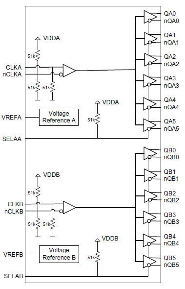
The 8P34S2106 is a high-performance, low-power, differential dual 1:6 LVDS output 1.8V/2.5V fanout buffer. The device is designed for the fanout of high-frequency, very low additive phase-noise clock and data signals. Two independent buffer channels are available, each channel has six low-skew outputs. High isolation between channels minimizes noise coupling. AC characteristics such as propagation delay are matched between channels. Guaranteed output-to-output and part-to-part skew characteristics make the 8P34S2106 ideal for clock distribution applications demanding well-defined performance and repeatability. The device is characterized to operate from a 1.8V/2.5V power supply. The integrated bias voltage references enable easy interfacing of AC coupled signals to the device inputs.
特性
- Dual 1:6 low skew, low additive jitter LVDS fanout buffers
- Matched AC characteristics across both channels
- High isolation between channels
- Low power consumption
- Both differential CLKA, nCLKA and CLKB, nCLKB inputs accept
LVDS, LVPECL, and single-ended LVCMOS levels - Maximum input clock frequency: 2GHz
- Output amplitudes: 350mV, 500mV (selectable)
- Output bank skew: 10ps typical
- Output skew: 20ps typical
- Low additive phase jitter, RMS: < 45fs typical,
(fREF = 156.25MHz, 12kHz to 20MHz) - Full 1.8V and 2.5V supply voltage mode
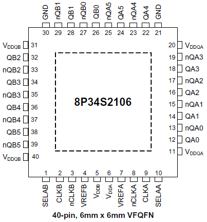
- Lead-free (RoHS 6), 40-lead VFQFN packaging
- -40 °C to 85 °C (Tc ≤ 105 °C) operating temperature range
产品对比
应用
- Clock distribution
设计和开发
模型
ECAD 模块
点击产品选项表中的产品,查找 SamacSys 中的原理图符号、PCB 足迹和 3D CAD 模型。点击产品选项表中的产品,查找 SamacSys 中的原理图符号、PCB 足迹和 3D CAD 模型。

产品选项
当前筛选条件
视频和培训
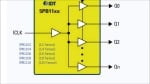
5PB11xx Ultra Low Jitter LVCMOS Buffers
Description
This video presentation will introduce users to IDT's 1.8 V LVDS clock fanout buffer family offering high-performance AC characteristics similar to that of 3.3 V devices. The new low-voltage fanout buffers enable customers to save up to 60% power and heat dissipation without sacrificing accuracy, bit error rates, or functionality.
Reducing power consumption is a key objective for many electronic designs, especially in high-performance systems. High-speed AC performance previously required the selection of high-power consumption IC solutions. With IDT's 1.8V differential clock buffer family, designers can now get both: excellent AC performance and low power consumption.
The IDT 8P34S family devices are currently sampling to qualified customers and are available in 16- to 40-lead VFQFN packages. Customers may select from the IDT 8P34S1102i (2 output), 8P34S1204i (4 output), 8P34S1106i (6 output), 8P34S1208i (8 output), and 8P34S1212i (12 output) devices. Presented by Vik Chaudhry, Marketing Manager at IDT. For more information visit our RF Buffer page.
Transcript
My name is Vick Chaudhry, I'm marketing manager for Timing Division at IDT. In this presentation I'll talk about a new family of 1.8 volt buffers from IDT, and we'll show its benefits and features. Reducing power consumption is a clear objective for many new designs especially in high-performance systems. With these new 1.8 volt buffers, designers can now get both excellent performance as well as low-power consumption.
This family of buffers consists of five devices. The device function is simple. It distributes a differential clock signal to multiple low skew outputs. Inputs and outputs are at LVDS levels. The family supports devices with two, four, six, eight, and twelve LVDS outputs. Despite the 1.8 volt supply voltage, the performance of these devices is comparable to buffers that supply voltage of 3.3 volts. This family allows for easy migration from IDTs existing 3.3 volt or 2.5 volt buffers to 1.8 volt buffers because these devices are function and footprint compatible with each other.
Let's have a look at the key characteristics of this new low-power family. The signal isolation is in the range of 18 dBs; which is a state of the art for clock devices. The excellent on-chip signal isolation helps achieve high signal to noise figures, and it simplifies or avoids external filtering. New devices have additive phase noise as low as 40 femtoseconds thus keeping the bit error rates low. The fast rise and fall time supports interfacing to converters with high sample rates, PHYs, and other high-speed logic. These devices can be used in applications with top frequencies up to 1.2 GHz
Now, we are looking at the main benefit, reduction of power consumption. Compared with function and performance comparable parts with 3.3 volt supplies, these new devices can reduce power by almost 60% while maintaining the same level of performance.
The standard application for low-power clock family is the distribution of differential signals. Each device generates multiple low phase-noise and low skew copies of the input signal. Because the new device utilizes a fully static design the distribution of NRCs data signals is fully supported. This performance and low-power characteristics is applicable to a wide range of equipment; such as wireless equipment, high-end and mid range routers, networking and switching equipment, storage and high-performance computing equipment. The packaging for all these devices is a standard QFN package and the sizes range from small 3x3 mm to 5x5 mm footprint.
Here is a summary of the main features and functions. These devices have two, four, six, eight, and twelve LVDS outputs. Several devices such as four, eight, and twelve output versions have two inputs with an internal multiplexer for signal selection. All devices have internal voltage generator for sound biasing inputs and AC coupled interphases. The output rise time or fall time is faster than 200 picoseconds, and the additive jitter is as low as 40 femtoseconds.
You will find more information related to these parts available on the IDT website. Data sheets and IBIS models are available for these devices. Evaluation boards are also available. IDT engineering team offers a schematic review to make sure that interfaces, signal termination, etc. are correctly done. Several application notes related to the interfacing between different Input/output levels and logic levels are available through the website. Please visit us at the IDT website for additional information.

Video List
新闻和博客
| IDT 扩展 1.8 V RF 双通道定时系列 提供高性能、低功耗的缓冲设备 | 新闻 | 2016年11月28日 |