概览
描述
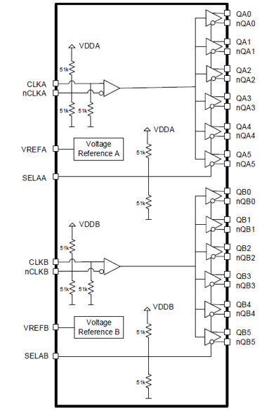
The 8P34S2106A is a high-performance, low-power, differential dual 1:6 LVDS output 1.8V/2.5V fanout buffer. The device is designed for the fanout of high-frequency, very-low additive phase noise clock and data signals. Two independent buffer channels are available, each channel has six low-skew outputs. High isolation between channels minimizes noise coupling. AC characteristics such as propagation delay are matched between channels. Guaranteed output-to-output and part-to-part skew characteristics make the 8P34S2106A ideal for clock distribution applications demanding well-defined performance and repeatability. The device is characterized to operate from a 1.8V/2.5V power supply. The integrated bias voltage references enable easy interfacing of AC-coupled signals to the device inputs. The device supports fail-safe operation, it can handle DC levels up to 2.5V on its input pins while the device is powered down with very low leakage currents and doesn’t impact long-term reliability.
特性
- Dual 1:6 low skew, low additive jitter LVDS fanout buffers
- Matched AC characteristics across both channels
- High isolation between channels
- Low power consumption
- Both differential CLKA, nCLKA and CLKB, nCLKB inputs accept LVDS, LVPECL, and single-ended LVCMOS levels
- Maximum input clock frequency: 2GHz
- Output amplitudes: 350mV, 500mV (selectable)
- Output bank skew: 10ps typical
- Output skew: 20ps typical
- Low additive phase jitter, RMS: < 30fs typical, (fREF = 156.25MHz, 12kHz to 20MHz)
- Full 1.8V and 2.5V supply voltage mode
- Lead-free (RoHS 6), 40-lead VFQFN packaging
- -40 °C to 85 °C (Tc ≤ 105 °C) operating temperature range
- Supports fail-safe operation
产品对比
应用
设计和开发
模型
ECAD 模块
点击产品选项表中的产品,查找 SamacSys 中的原理图符号、PCB 足迹和 3D CAD 模型。点击产品选项表中的产品,查找 SamacSys 中的原理图符号、PCB 足迹和 3D CAD 模型。

产品选项
当前筛选条件