概览
描述
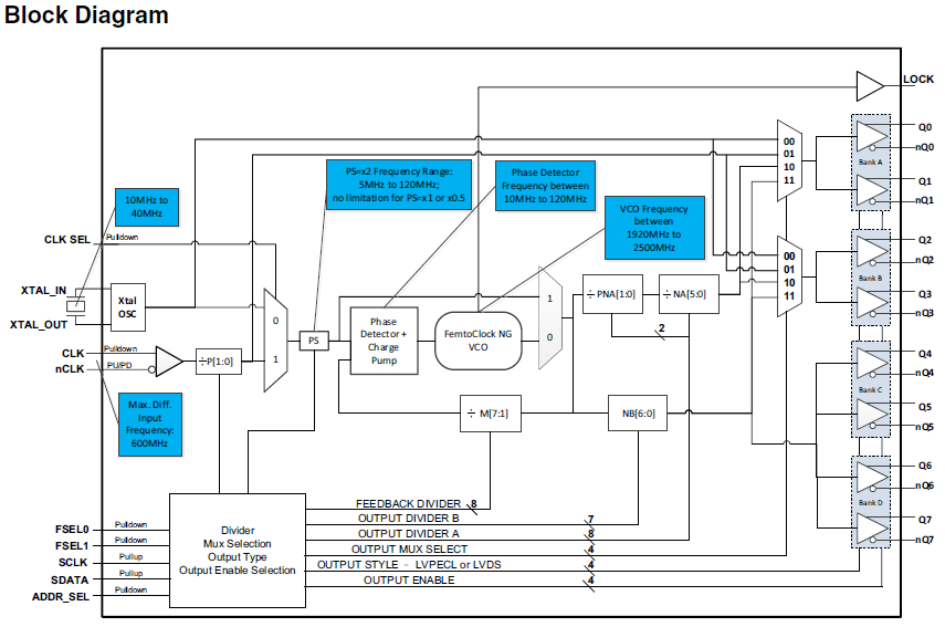
The 8T49N028 is a low RMS phase jitter clock synthesizer with selectable internal crystal oscillator or external clock references and eight outputs, configurable as either LVDS, LVPECL, or high impedance.
After power up, two frequency select pins determine one of up to four different sets of factory preprogrammed crystal or input frequency and output frequency configurations. From a single input reference, as many as three different output frequencies may be selected for the output banks: two of these frequencies can be generated by the internal crystal oscillator, and/or external clock pre-divider, and/or A output divider, and/or B output divider. The third output frequency is from the B output divider. Device pre-programming can be overwritten through the provided I2C interface.
The specific internal register settings for each of the four frequency sets are specified by a Renesas order code. Custom codes can be provided by contacting Renesas.
特性
- Fourth-generation FemtoClock™ NG PLL technology
- Eight selectable LVPECL or LVDS outputs (bank selectable, two output channels per bank)
- CLK, nCLK input pair can accept the following differential input levels: LVPECL, LVDS, HCSL
- FemtoClock NG VCO range: 1.92GHz to 2.5GHz
- Bank A and B output frequencies are mux selectable from internal crystal oscillator, reference clock input, output divider A, or output divider B
- Clock from OUTPUT DIVIDER A, RMS phase jitter at 156.25MHz
(12KHz to 20MHz): 225fs (typical) - Clock from OUTPUT DIVIDER B, RMS phase jitter at 156.25MHz
(12KHz to 20MHz): 219fs (typical) - Clock from OUTPUT DIVIDER B, RMS phase jitter at 156.25MHz
(10kHz to 1MHz): 165fs (typical) - Full 2.5V or 3.3V power supply
- I2C programming interface
- PCI Express (2.5Gb/S), Gen2 (5Gb/s), and Gen3 (8Gb/s) jitter compliant
- -40 °C to 85 °C ambient operating temperature
- Lead-free (RoHS 6) packaging
产品对比
应用
设计和开发
模型
ECAD 模块
点击产品选项表中的产品,查找 SamacSys 中的原理图符号、PCB 足迹和 3D CAD 模型。点击产品选项表中的产品,查找 SamacSys 中的原理图符号、PCB 足迹和 3D CAD 模型。

产品选项
当前筛选条件