概览
描述
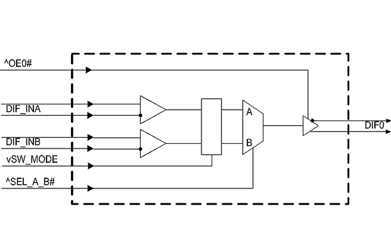
The 9DMV0131 is a member of Renesas' SOC-Friendly 1.8 V Very-Low-Power (VLP) PCIe Gen1–5 family. The output has an OE# pin for optimal system control and power management. The part provides asynchronous or glitch-free switching modes.
特性
- LP-HCSL output; saves 2 resistors compared to standard HCSL output
- 1.8 V operation; 12 mW typical power consumption
- Selectable asynchronous or glitch-free switching; allows the mux to be selected at power up even if both inputs are not running, then transition to glitch-free switching mode
- Spread spectrum compatible; supports EMI reduction
- OE# pin; supports DIF power management
- HCSL differential inputs; can be driven by common clock sources
- 1 MHz to 200 MHz operating frequency
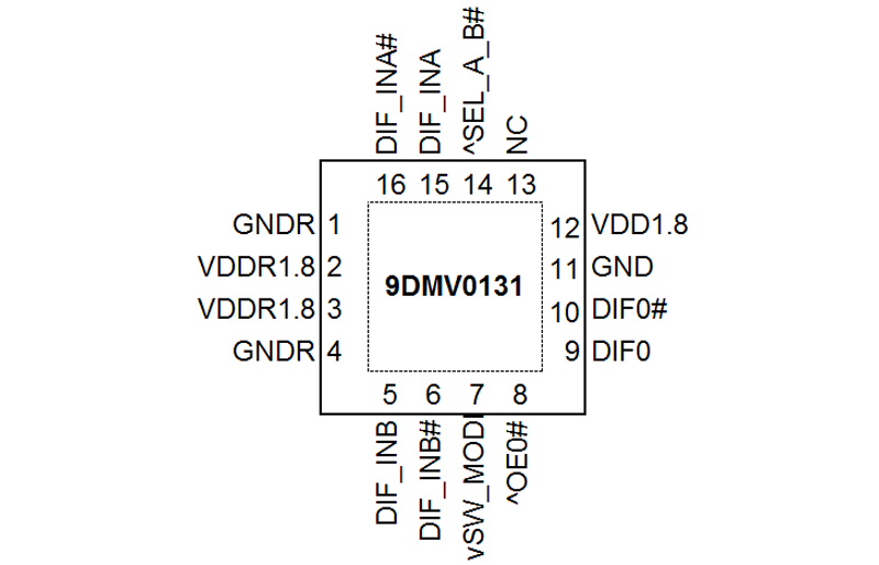
- Space saving 3x3 mm 16-pin VFQFPN; minimal board space
产品对比
应用
设计和开发
模型
ECAD 模块
点击产品选项表中的产品,查找 SamacSys 中的原理图符号、PCB 足迹和 3D CAD 模型。点击产品选项表中的产品,查找 SamacSys 中的原理图符号、PCB 足迹和 3D CAD 模型。

产品选项
当前筛选条件
视频和培训
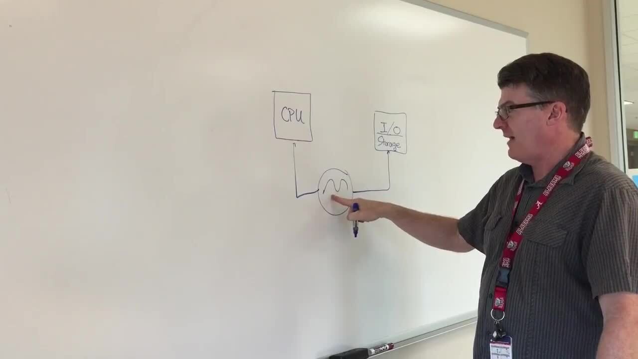
PCIe Clocking Architectures (Common and Separate)
This is the first video in our PCIe series. In this video, we define PCIe architectures, focusing on common and separate clock architectures. Watch the rest of the video series below where Ron will cover the impact of different timing architectures.
Watch the Video Series Below
Video List