概览
描述
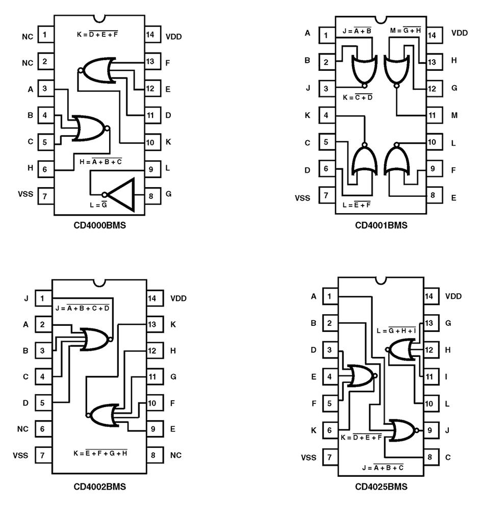
The CD4000BMS (dual 3 plus inverter), CD4001BMS (quad 2-input), CD4002BMS (dual 4-input), and CD4025BMS (triple 3-input) NOR gates provide the system designer with direct implementation of the NOR function and supplement the existing family of CMOS gates. All inputs and outputs are buffered. The CD4000BMS, CD4001BMS, CD4002BMS, and the CD4025BMS are supplied in these 14-lead outline packages: Braze Seal DIP H4X and H4Q, Frit Seal DIP H1B, and Ceramic Flatpack H3W.
特性
- High-voltage types (20V rating)
- Propagation delay time = 60ns (typ.) at CL = 50pF, VDD = 10V
- Buffered inputs and outputs
- Standard symmetrical output characteristics
- 100% tested for maximum quiescent current at 20V
- 5V, 10V and 15V parametric ratings
- Maximum input current of 1µA at 18V over full package temperature range; 100nA at 18V and +25 °C
- Noise margin (over full package temperature range):
- 1V at VDD = 5V
- 2V at VDD = 10V
- 2.5V at VDD = 15V
- Meets all requirements of JEDEC tentative standards No. 13B, "Standard Specifications for Description of "B" Series CMOS Device's
产品对比
应用
文档
相关文档
请登录后开启订阅
|
|
|
|
|---|---|---|
| 类型 | 文档标题 | 日期 |
| 数据手册 | PDF 404 KB | |
| 宣传手册 | PDF 467 KB | |
| 涨价通告 | PDF 360 KB | |
| 产品咨询 | PDF 499 KB | |
| 产品变更通告 | PDF 230 KB | |
5 items
|
||
设计和开发
模型
ECAD 模块
点击产品选项表中的 CAD 模型链接,查找 SamacSys 中的原理图符号、PCB 焊盘布局和 3D CAD 模型。如果符号和模型不可用,可直接在 SamacSys 请求该符号或模型。

产品选项
当前筛选条件