概览
描述
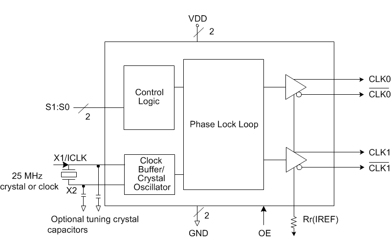
The IDT5V41315 is a PCIe Gen1/2/3 clock synthesizer suitable for use in both Common-Clocked and Separate Reference clock with No Spread (SRNS) timing architectures. The IDT5V41315 uses a 25MHz input to generate 4 different output frequencies. The output frequency is selectable via select pins.
特性
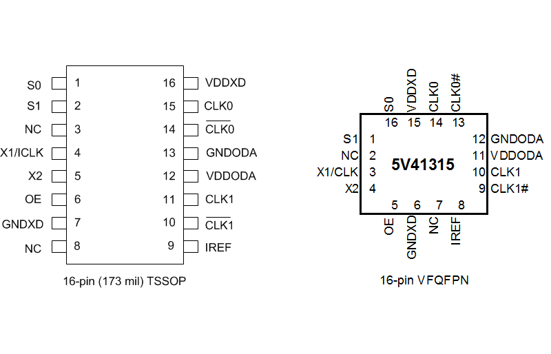
- 16-pin TSSOP or VFQFPN package; small board footprint
- Outputs can be terminated to LVDS; can drive a wider variety of devices
- OE control pin; greater system power management
- Industrial temperature range available; supports demanding embedded applications
- Cycle-to-cycle jitter: 80ps
- Output-to-output skew: <50 ps
- PCIe Gen2 phase jitter: <3.0ps RMS (Common Clock)
- PCIe Gen3 phase jitter: <1.0ps RMS (Common Clock)
- Low Phase Noise: 12KHz to 20MHz <6ps RMS
产品对比
应用
设计和开发
模型
ECAD 模块
点击产品选项表中的 CAD 模型链接,查找 SamacSys 中的原理图符号、PCB 焊盘布局和 3D CAD 模型。如果符号和模型不可用,可直接在 SamacSys 请求该符号或模型。

产品选项
当前筛选条件
视频和培训
PCIe Clocking Architectures (Common and Separate)
This is the first video in our PCIe series. In this video, we define PCIe architectures, focusing on common and separate clock architectures. Watch the rest of the video series below where Ron will cover the impact of different timing architectures.
Watch the Video Series Below
Video List