概览
描述
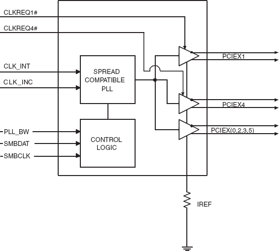
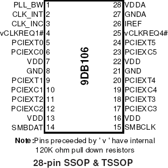
The 9DB106 zero-delay buffer supports PCIe Gen1 and Gen2 clocking requirements. The 9DB106 is driven by a differential SRC output pair from an IDT CK410/CK505-compliant main clock generator. It attenuates jitter on the input clock and has a selectable PLL bandwidth to maximize performance in systems with or without Spread-Spectrum clocking. An SMBus interface allows control of the PLL bandwidth and bypass options, while 2 clock request (CLKREQ#) pins make the 9DB106 suitable for Express Card applications.
特性
- 6 - 0.7 V current mode differential output pairs (HCSL)
- CLKREQ# pin for outputs 1 and 4/ supports Express Card applications
- PLL or bypass mode/PLL can dejitter incoming clock
- Selectable PLL bandwidth/minimizes jitter peaking in downstream PLL's
- Spread Spectrum Compatible/tracks spreading input clock for low EMI
- SMBus Interface/unused outputs can be disabled
- Cycle-to-cycle jitter < 50 ps
- Output-to-output skew < 50 ps
产品对比
应用
设计和开发

产品选项
当前筛选条件
视频和培训
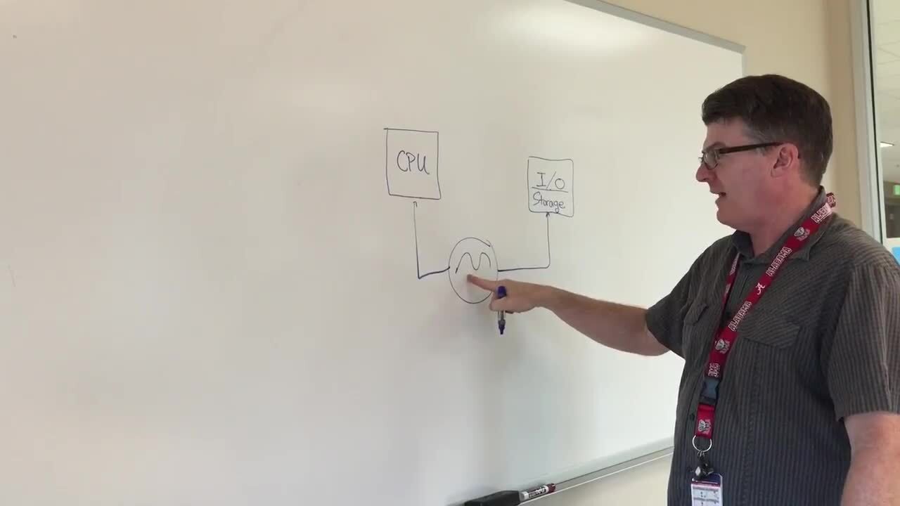
PCIe Clocking Architectures (Common and Separate)
This is the first video in our PCIe series. In this video, we define PCIe architectures, focusing on common and separate clock architectures. Watch the rest of the video series below where Ron will cover the impact of different timing architectures.
Watch the Video Series Below
Video List