概览
描述
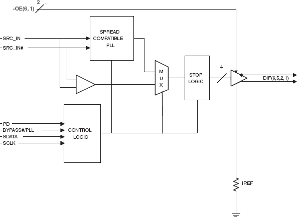
The 9DB403 is compatible with the Intel DB400v2 Differential Buffer Specification. This buffer provides 4 PCI Express® Gen2 clocks. The 9DB403 is driven by a differential output pair from a CK410B+, CK505 or CK509B main clock generator.
特性
- 4 - 0.7 V current-mode differential output pairs
- Supports zero delay buffer mode and fanout mode
- Bandwidth programming available
- 50-100 MHz operation in PLL mode
- 50-400 MHz operation in Bypass mode
- Spread spectrum modulation tolerant, 0 to -0.5% down spread and +/- 0.25% center spread.
- Supports undriven differential outputs in PD# and SRC_STOP# modes for power management.
- Outputs cycle-cycle jitter < 50 ps
- Outputs skew: 50 ps
- Phase jitter: PCIe Gen1 < 86 ps peak to peak
- Phase jitter: PCIe Gen2 < 3.0/3.1 ps rms
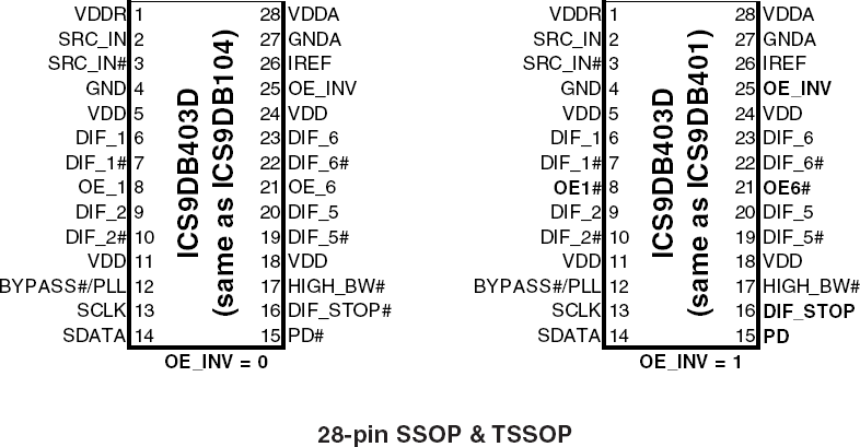
- 28-pin SSOP/TSSOP package
- Available in RoHS compliant packaging
- Supports Commercial (0 to +70°C) and Industrial (-40 to +85°C) temperature ranges
产品对比
应用
设计和开发
模型
ECAD 模块
点击产品选项表中的 CAD 模型链接,查找 SamacSys 中的原理图符号、PCB 焊盘布局和 3D CAD 模型。如果符号和模型不可用,可直接在 SamacSys 请求该符号或模型。

产品选项
当前筛选条件
视频和培训
PCIe Clocking Architectures (Common and Separate)
This is the first video in our PCIe series. In this video, we define PCIe architectures, focusing on common and separate clock architectures. Watch the rest of the video series below where Ron will cover the impact of different timing architectures.
Watch the Video Series Below
Video List