概览
描述
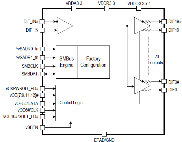
The 9QXL2001B is a 20-output very-low-additive phase jitter fanout buffer for PCIe Gen 4, Gen 5, and UPI applications. The 9QXL2001B provides two methods to control output enables; standard OE# pins and SMBus enable bits, or a simple 3-wire serial interface that is independent of the SMBus. The OE Control Mode is set via a hardware strap. It offers integrated terminations for 85Ω transmission lines.
特性
- Traditional 8 OE# pins allow hardware control of 8 outputs and 20 SMBus bits allow software control of each output
- Simple 3-wire Side-Band Interface allows real-time control of all 20 outputs
- Outputs remain Low/Low when powered up with a floating input clock
- Low-Power HCSL (LP-HCSL) outputs reduce device power consumption by 50%
- Zo = 85Ω outputs eliminate 80 resistors, saving 130mm2 of area
- 9 selectable SMBus addresses
- Spread spectrum compatible
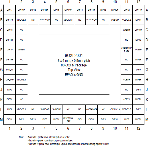
- 6mm × 6mm dual-row 80-GQFN
产品对比
应用
设计和开发

产品选项
当前筛选条件
视频和培训
PCIe Gen5 Clock Buffers
Introducing Renesas’ enhanced PCIe clock buffer family. These PCIe Gen5 clock buffers offer fanout and zero-delay operating modes, supporting both legacy systems and the most complex timing trees within a single device. Unlike many existing solutions, whose performance limitations force their use in fanout buffer mode, these clock buffers meet both PCIe Gen5 and prominent CPU-specific phase jitter requirements in all operating modes. The extremely low 50fs rms PCIe Gen5 additive phase jitter enables multi-level cascading within the strict PCIe Gen5 jitter budget. Renesas’ high-performance oscillators and clock generators provide an ideal clock source for the enhanced PCIe clock buffer family.
For more information about these PCIe Gen5 clock buffers, visit the PCIe timing page.
Video List