概览
描述
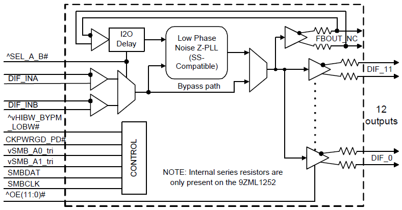
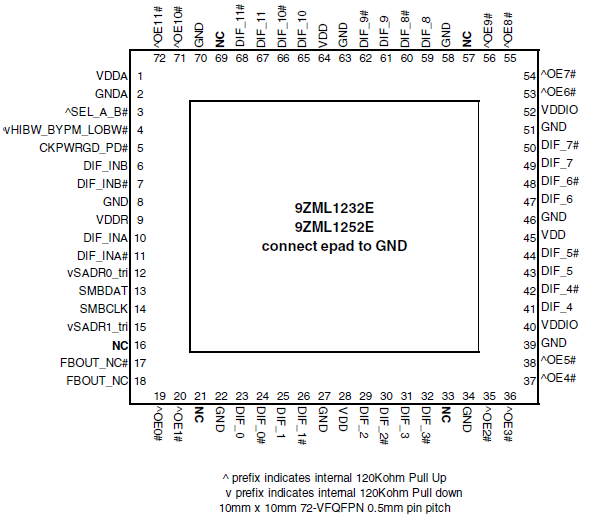
The 9ZML1232E is a second-generation 2-input/12-output differential mux for Intel Purley and newer platforms. It exceeds the demanding DB1200ZL performance specifications and is backward compatible with the 9ZML1232B. The device utilizes Low Power HCSL-compatible outputs to reduce power consumption and termination resistors. It is suitable for PCI Express Gen 1-4 or QPI/UPI applications, and provides two configurable low-drift I2O settings, one for each input channel, to allow I2O tuning for various topologies.
特性
- 2 configurable low-drift I2O delays up to 2.9ns; maintain transport delay for various topologies
- LP-HCSL outputs; eliminate 24 resistors
- 9 selectable SMBus addresses; multiple devices can share the same SMBus segment
- Separate VDDIO for outputs; allows maximum power savings
- PLL or Bypass Mode; PLL can de-jitter incoming clock
- Hardware or software-selectable PLL BW; minimizes jitter peaking in downstream PLLs
- Spread spectrum compatible; tracks spreading input clock for EMI reduction
- SMBus interface; software can modify device settings without hardware changes
- 10mm x 10mm 72-QFN package; small board footprint
产品对比
应用
设计和开发
开发板与套件
评估
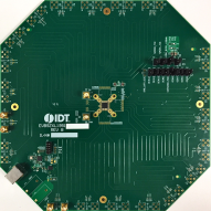
EVK9ZXL1951D
有效
Evaluation Kit for 19-Output DB1900Z for PCIe Gen1-4 and QPI/UPI
The evaluation board is designed to help the customer evaluate the 9ZXL1951D. The device is programmable through an SMBus interface. The user guide details the board set and connection, as well as the companion Graphical User Interface (GUI) installation for communicating with the device. The...
Recommended Documents:
模型
ECAD 模块
点击产品选项表中的 CAD 模型链接,查找 SamacSys 中的原理图符号、PCB 焊盘布局和 3D CAD 模型。如果符号和模型不可用,可直接在 SamacSys 请求该符号或模型。

产品选项
当前筛选条件
视频和培训
PCIe Gen5 Clock Buffers
Introducing Renesas’ enhanced PCIe clock buffer family. These PCIe Gen5 clock buffers offer fanout and zero-delay operating modes, supporting both legacy systems and the most complex timing trees within a single device. Unlike many existing solutions, whose performance limitations force their use in fanout buffer mode, these clock buffers meet both PCIe Gen5 and prominent CPU-specific phase jitter requirements in all operating modes. The extremely low 50fs rms PCIe Gen5 additive phase jitter enables multi-level cascading within the strict PCIe Gen5 jitter budget. Renesas’ high-performance oscillators and clock generators provide an ideal clock source for the enhanced PCIe clock buffer family.
For more information about these PCIe Gen5 clock buffers, visit the PCIe timing page.
Video List