概览
描述
8V19N882 是一款完全集成的 FemtoClock® 射频采样时钟发生器和抖动衰减器,是高性能的时钟解决方案,用于无线基站无线电设备板的调理和频率/相位管理。 该器件经过优化,可提供出色的相位噪声性能,满足 4G、5G、无线电(包括毫米波)实施的要求。
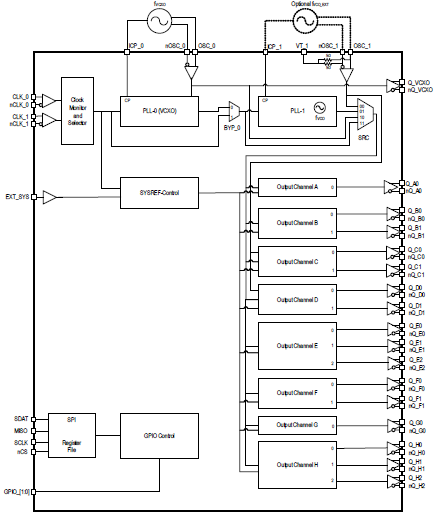
该器件支持 JESD204B(子类 0 和 1)和 JESD204C。 两级 PLL 架构支持抖动衰减和倍频。 第一级 PLL 是抖动衰减器,使用外部 VCXO 来实现最佳的相位噪声特性。 第二级 PLL 锁定第一个 PLL 输出信号并合成目标频率。 第二级 PLL 可使用内部或外部高频 VCO。
该器件从所选 VCO 生成高频时钟和低频同步信号(SYSREF)。 SYSREF 信号在内部与时钟信号同步。 集成的信号延迟模块可用于实现相位对齐、系统基准信号和时钟信号之间的受控相位偏移,以及对齐/延迟单个输出信号。 对两个冗余输入进行活动监控。 该器件提供了四种可选的时钟切换模式,用于处理时钟输入故障情况。 增加了自动锁定、单独可编程的输出分频器和相位调整功能,以提高灵活性。
该器件通过 3/4 线 SPI 接口进行配置,并通过内部寄存器和 GPIO[1:0] 输出报告锁定和信号丢失状态。 内部状态位变化也可以通过 GPIO 输出报告。
有关评估板和材料的信息,请联系您当地的销售代表。
特性
- 高性能时钟 RF 采样时钟发生器和时钟抖动衰减器,支持JESD204B/C
- 低相位噪声:-144.7dBc/Hz(800kHz 偏移;491.52MHz)
- 积分相位噪声:74fs RMS(12kHz–20MHz,491.52MHz)
- 带内部和可选外部 VCO 的双 PLL 架构
- 8 个输出通道,共 16 个输出
- 可配置整数时钟分频器
- 时钟输出频率:高达 3932.16MHz(内部 VCO)和 6GHz(可选外部 VCO)
- 差分、低噪声 I/O
- 确定性相位延迟和集成相位延迟电路
- 冗余输入时钟架构,具有两个输入和监控器,以及保持和输入切换功能
- SPI 3/4 线配置接口
- 电源电压:1.8V、2.5V 和 3.3V
- 封装:76-VFQFN(9 × 9 mm²)
- 温度范围:-40°C 至 +105°C(电路板)
产品对比
应用
设计和开发
软件与工具
开发板与套件
评估
8V19N882-EVK
预览
8V19N882 Evaluation Kit
The evaluation kit supports the electrical evaluation process of the 8V19N882NVGI JESD204B/C clock jitter attenuator for all major device parameters including phase noise, spurious attenuation, clock frequency, output skew, phase alignment, device timing and the signal waveform. The device is a...
Recommended Documents:
模型
ECAD 模块
点击产品选项表中的 CAD 模型链接,查找 SamacSys 中的原理图符号、PCB 焊盘布局和 3D CAD 模型。如果符号和模型不可用,可直接在 SamacSys 请求该符号或模型。

产品选项
当前筛选条件
视频和培训
8V19N880, 8V19N882 Low-Power 4G & 5G RF Clock Jitter Attenuators
The 8V19N880 and 8V19N882 JESD204B/C clock jitter attenuators deliver low phase noise and exceptional jitter performance as low as 74fs RMS and -90dB spurious attenuation for mission-critical industrial data converter applications in wireless radio, test and measurement, instrumentation, and high-performance imaging. They support frequencies up to 3932.16MHz (up to 6GHz with an external VCO) and feature 16 and 18 integrated differential outputs to deliver a first-in-class balance of high performance, low voltage and low power consumption with 1.8V support.
Video List
Demystifying 5G Video Series
Rohde & Schwarz's Demystifying 5G video series discusses main topics related to 5G including new technology components, procedures and testing challenges.