概览
描述
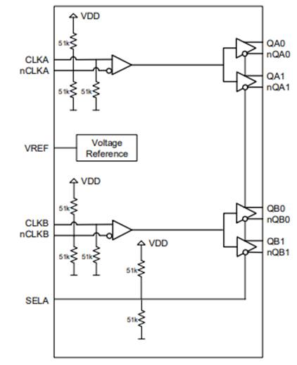
The 8P34S2102 is a high-performance, low-power, differential dual 1:2 LVDS output, 1.8V/2.5V fanout buffer. The device supports fail-safe operation and is designed for the fanout of high-frequency, very low additive phase-noise clock and data signals. Two independent buffer channels are available. Each channel has two low-skew outputs. High isolation between channels minimizes noise coupling. AC characteristics such as propagation delay are matched between channels. Guaranteed output-to-output and part-to-part skew characteristics make the 8P34S2102 ideal for those clock distribution applications demanding well-defined performance and repeatability. The device is characterized to operate from a 1.8V or a 2.5V power supply. The integrated bias voltage references enable easy interfacing of AC-coupled signals to the device inputs.

特性
- Dual 1:2 low skew, low additive jitter LVDS fanout buffers
- Matched AC characteristics across both channels
- High isolation between channels
- Low power consumption
- Both differential CLKA, nCLKA and CLKB, nCLKB inputs accept LVDS, LVPECL and single-ended LVCMOS levels
- Maximum input clock frequency: 2.0GHz
- Output amplitudes: 350mV, 500mV (selectable)
- Output bank skew: 5ps typical
- Output skew: 30ps typical
- Low additive phase jitter, RMS: 40fs typical (fREF = 156.25MHz, 12kHz to 20MHz)
- Full 1.8V / 2.5V supply voltage mode
- Lead-free (RoHS 6), 16-lead VFQFN packaging
- -40°C to 85°C (Tc ≤ 105°C) operating temperature range
产品对比
应用
设计和开发

产品选项
当前筛选条件
视频和培训
新闻和博客
| IDT 扩展 1.8 V RF 双通道定时系列 提供高性能、低功耗的缓冲设备 | 新闻 | 2016年11月28日 |