概览
描述
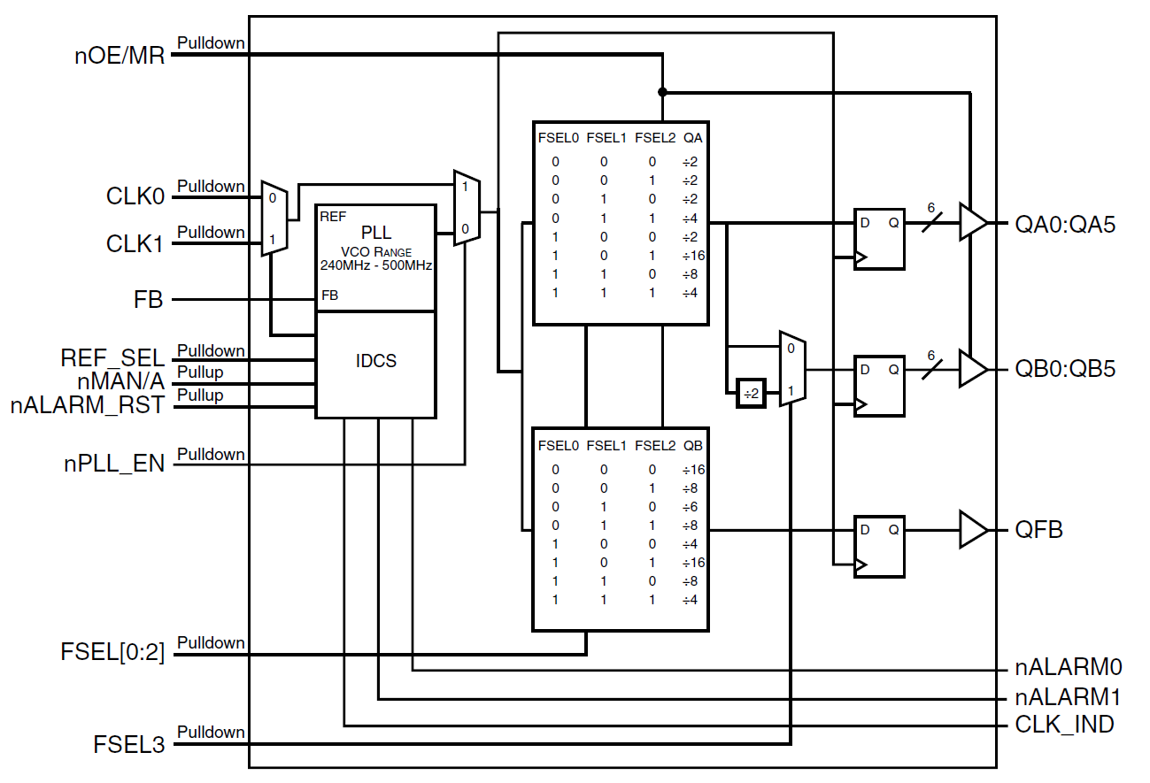
The 879893I is a PLL clock driver designed specifically for redundant clock tree designs. The device receives two LVCMOS/LVTTL clock signals from which it generates 12 new LVCMOS/LVTTL clock outputs. External PLL feedback is used to also provide zero delay buffer performance. The 879893I Intelligent Dynamic Clock Switch (IDCS) circuit continuously monitors both input CLK signals. Upon detection of a failure (CLK stuck HIGH or LOW for at least 1 period), the nALARM for that CLK will be latched (LOW). If that CLK is the primary clock, the IDCS will switch to the good secondary clock and phase/frequency alignment will occur with minimal output phase disturbance.
特性
- Twelve LVCMOS/LVTTL outputs (two banks of six outputs)
- One QFB feedback clock output
- Selectable CLK0 or CLK1 LVCMOS/LVTTL clock inputs
- CLK0, CLK1 supports the following input types:
- LVCMOS, LVTTL
- Automatically detects clock failure
- IDCS on-chip intelligent dynamic clock switch
- Maximum output frequency: 200MHz
- Output skew: 50ps (maximum), within bank
- Cycle-to-cycle (FSEL3=0, VDD=3.3V±5%): 150ps (maximum)
- Smooth output phase transition during clock fail-over switch
- Full 3.3V or 2.5V supply modes
- -40°C to 85°C ambient operating temperature
- Available in lead-free (RoHS 6) package
产品对比
应用
设计和开发
模型
ECAD 模块
点击产品选项表中的 CAD 模型链接,查找 SamacSys 中的原理图符号、PCB 焊盘布局和 3D CAD 模型。如果符号和模型不可用,可直接在 SamacSys 请求该符号或模型。

产品选项
当前筛选条件