概览
描述
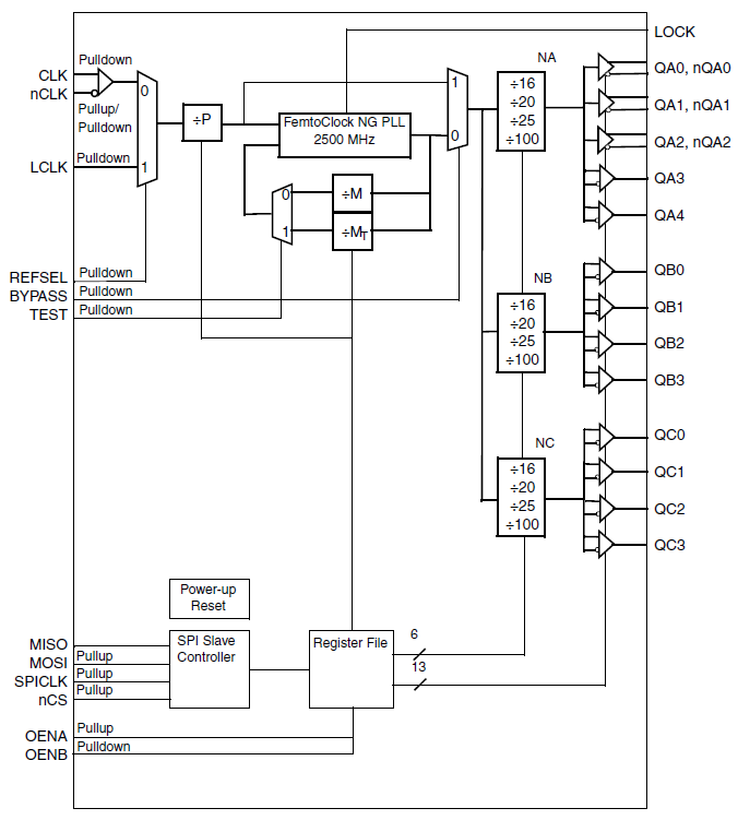
The 8V44N4614 is a FemtoClock® NG clock generator. The device has been designed for frequency generation in high-performance systems such as wireless baseband boards, for instance, to drive the reference clock inputs of processors, PHY, switches, and SerDes devices. The device is very flexible in frequency programming. It allows for the generation of clock frequencies of 156.25MHz, 125MHz, 100MHz, and 25MHz individually at three output banks. One output bank supports configurable LVDS and LVPECL, and the other two output banks support LVCMOS output levels. All outputs are synchronized on the incident rising edge, regardless of the selected output frequency. Selective single-ended LVCMOS outputs can be configured to invert the output phase, effectively forming differential LVCMOS output pairs for noise reduction. The PLL reference signal is either a 25MHz, 50MHz, 100MHz, or 200MHz differential or single-ended clock.
The device is optimized to deliver excellent period and cycle-to-cycle jitter performance, combined with good phase noise performance, and high power supply noise rejection.
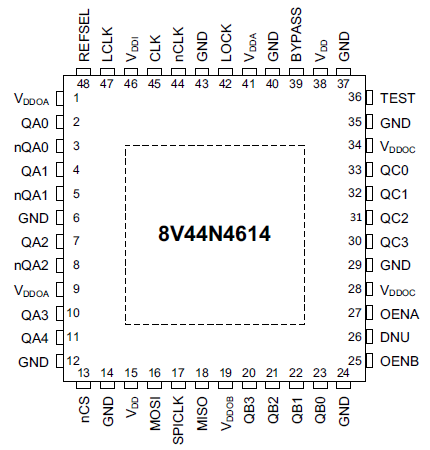
The clock generator is configured through an SPI serial interface. Outputs can be configured to any of the available output frequencies. Two hardware pins are available for selecting pre-set output enable/disable configurations. In each of these pre-set configurations, each output can be enabled/disabled individually. A separate test mode is available for an increase or decrease of the output frequencies in 19.53125ppm steps independent of the input frequency. The device is packaged in a lead-free (RoHS 6) 48-lead VFQFN package. The extended temperature range supports wireless infrastructure, telecommunication, and networking end equipment requirements.
特性
- Clock generator for wireless baseband systems
- Drives reference clock inputs of processors, PHY, switches, and SerDes devices
- FemtoClock NG technology
- Three low-skew, differential LVDS, LVPECL configurable clock outputs
- Ten low-skew, LVCMOS/LVTTL clock outputs
- Input: 200MHz, 100MHz, 50MHz, 25MHz single-ended (LVCMOS) or differential reference clock (LVDS, LVPECL)
- Output clocks support 156.25MHz, 125MHz, 100MHz, and 25MHz
- Individual output disable (high-impedance)
- Two sets of output enable configurations
- PLL lock detect output
- Test mode with frequency margining with 19.53125ppm steps
(range ±507.8125ppm) - LVCMOS (1.8V, JESD8-7A) compatible SPI programming interface
- Cycle-to-Cycle jitter: 10ps (typical)
- RMS period jitter: 1.6ps (typical)
- Phase noise (12kHz to 20MHz): 0.40ps (typical)
- 3.3V core and output supply
- -40 °C to +85 °C ambient operating temperature
- Lead-free (RoHS 6) 48-lead VFQFN packaging
产品对比
应用
设计和开发
模型
ECAD 模块
点击产品选项表中的 CAD 模型链接,查找 SamacSys 中的原理图符号、PCB 焊盘布局和 3D CAD 模型。如果符号和模型不可用,可直接在 SamacSys 请求该符号或模型。

产品选项
当前筛选条件