What is PR40?
PR40 is an advanced complementary bipolar process on bonded-SOI substrates that is used to optimize performance for high voltage precision analog applications. Reducing parasitic leakage, minimizing noise and avoiding latch-up allows optimization for high voltage, low power, stability, and design flexibility. The PR40 process is in volume production under MIL-PRF-38535 certification in the Palm Bay, Florida wafer fabrication facility.
Application Challenges
For semiconductors, medical and industrial applications often present difficult operating environments with extreme temperature ranges, high levels of ESD and high sensitivity to electronic noise. These applications demand robust, high-voltage precision circuits for data acquisition and signal processing. The combination of high accuracy, high voltage, and low-noise requirements, plus the need to deploy in harsh operating environments, make it extremely difficult to create precision analog front-end components and circuits that can handle all of the challenges.
These challenges range across a wide spectrum of high-performance applications such as:
- Medical imaging and instrumentation
- Process control (I/O modules)
- Precision instrumentation and test systems
- Spectral analysis equipment
- Thermocouples
- Bio-analyzers
- ATE and data acquisition
The design of precision analog front-end circuitry can be especially challenging for applications that use high-impedance sensors. These devices are inherently more prone to capacitive and inductive noise pick-up, and typically have higher noise sensitivity, which can make it difficult to achieve repeatability of readings and overall stability of the design. For example, many industrial systems using optical imaging, photodiodes, piezoelectric sensors, piezoresistive pressure transducers, PH sensors, or gas meters must be able to provide fast and accurate readings under often very harsh operating conditions for real-time process monitoring and control applications.
As discussed in this article, solving these challenges requires a fundamental bottom-up approach that starts with the use of advanced bipolar processes to design and manufacture products, such as precision op amps, instrumentation amps and bandgap voltage references. By leveraging fabrication techniques such as deep trench isolation and lateral device spacing to optimize noise performance and minimize parasitic leakage at the transistor level, this approach enables the designer to create very robust products that have very efficient power-to-bandwidth characteristics and can handle high-impedance inputs with speed, accuracy and low power usage.
Process Methodology Overview
The 40V complementary bipolar plus JFET (CBiFET) process known as PR40 was developed expressly for the development of robust products optimized for precision analog circuit applications. The process is fabricated on bonded silicon-on-insulator (BSOI) substrates and uses deep trench isolation (DTI) to build devices with complete dielectric isolation. The process features a core-bipolar foundation and optional device modules that are added as needed to facilitate product-specific, low-cost manufacturing. The PR40 process is currently being used to fabricate a range of low-noise precision op amps, instrumentation amps, current sense amps and bandgap voltage references for use in industrial, medical and other high-performance applications.
BSOI substrates offer a number of important advantages. These include robust devices with low parasitics that exhibit very predictable device performance characteristics and are free of latch-up in harsh environment applications. BSOI is a convenient isolation method for making complementary bipolar devices with significant area reduction compared to the junction-isolated devices that are typically used in high voltage analog circuits.
SOI uses layers of silicon-insulator-silicon in place of conventional silicon substrates. This allows for lower parasitic capacitance due to isolation from the bulk silicon. Deep trench dielectric isolation provides separation of devices to further minimize capacitance and reduce leakage current associated with diodes, transistors, etc. The reduced level of parasitics allow the designer to optimize power-to-bandwidth efficiency and reduce overall power consumption.
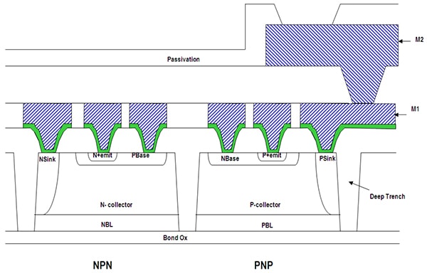
Cross-Section of PR40 NPN and PNP Devices
Avoiding Latch-up
Latch-up is one of the most problematic conditions that can result from an inadequate front-end analog design. In essence, latch-up is a particular type of short circuit that results from the inadvertent creation of a low impedance path between the power supply rails of an IC, which triggers a parasitic structure that disrupts the proper functioning of the part. A power cycle is typically required to correct the situation and latch-up can even lead to destruction of the part due to an overcurrent condition.
The parasitic structure that causes latch-up is equivalent to an unintentional thyristor that is acting across a PNP and an NPN transistor stacked next to each other. Latch-up occurs when one of the transistors is conducting and the other starts to conduct at the same time. Then, both transistors keep each other in saturation for as long as the structure is forward biased and current is flowing through it.
Latch-up can happen at any location where the underlying parasitic condition exists. For example, a spike of positive or negative voltage on an output or input pin of a digital chip that exceeds the rail voltage by more than a diode drop is a common cause of latch-up. Another cause is the supply voltage exceeding the absolute maximum rating, for instance from a transient spike in the power supply.
By using advanced fabrication processes such as BSOI, deep trench isolation and optimal lateral device separation, the PR40 process enables latch-up free circuit operation.
Maximizing Design Flexibility
To maximize design flexibility, the PR40 process features a full suite of precision analog devices including 40V low-noise NPN and vertical PNP bipolar devices, 40V P- and N-channel JFETs, 10V super-beta NPNs, and MOSFETs. In addition, the process offers a high BVebo lateral PNP device with high-beta, a buried Zener, and a well controlled Schottky diode. The process supports multiple levels of metal, as well as active area bonding.
The process is optimized to allow for consistent matching of devices, with both the NPN and PNP structures constructed in a similar fashion on a common subsurface base. Thin film resistors provide precision matching in relatively little area. The low temperature coefficient of the thin film makes it possible to achieve tighter specifications over wider operating temperatures. It offers an optimized high-density multilayer capacitor that provides additional design flexibility and minimizes die area. In terms of ESD protection, it offers superior ESD structures that easily achieve the minimum 2KV HBM targets and are typically in the 4KV - 6KV range.
These unique capabilities of the PR40 process provide the designer great flexibility for designing high-performance precision analog circuits. The exceptional device matching enables the design of very high precision amplifiers with minimal offset trim requirements. The absence of parasitic junction leakage over temperature combined with predictable device behavior enable high impedance input amplifiers with very low and stable input bias current behavior across their specified common mode voltage and four temperature ranges. Deep trench isolation results in very small device footprints enabling very efficient noise and power tradeoffs that result in low power designs with exceptional noise performance. Small devices combined with active area bonding and high density capacitors result in very dense circuits that enable 40V products in small footprint packages such as SOT23, uTDFN and MSOP.
Robust ESD Performance
Products designed on PR40 are also inherently radiation-tolerant and capable of delivering very robust ESD performance. In most analog front-end devices using conventional fabrication processes, it is very difficult to achieve good ESD characteristics while delivering high performance. Because products created with the PR40 process are fully dielectrically isolated using a mechanical process, any sensitivity to electromagnetic pulses has been completely eliminated. Also the use of subsurface transistors with deep junctions means less sensitivity to ionization radiation.
The Bottom Line
The use of advanced feature-rich complementary bipolar and BSOI fabrication processes, along with deep trench dielectric isolation, provides a very predictable and flexible foundation for designing robust, high-voltage, low-noise, low-power devices for use in precision analog front-end designs. Elimination of internal parasitic structures within the devices and inherent resistance to external ESD or radiation make these devices ideal for use throughout a wide range of industrial, medical and other applications that require high accuracy within difficult operating environments.
In addition, because it is a modular fabrication process with a wide range of features that can be incorporated for specific designs, the PR40 approach also improves both design flexibility, product cost and package size. Critical features needed for specific designs can be predictably modeled and efficiently integrated so as to minimize the size of the design while optimizing its performance for the target application.
The bottom line is that precision analog design will always present difficult challenges, especially for those applications that combine high-impedance sensors, high voltages, the need for high accuracy and exposure to harsh operating environments. The PR40 process lessens the difficulty by addressing all of these issues from the bottom up.