概览
描述
The 8V19N472 is a fully integrated FemtoClock NG Jitter Attenuator and Clock Synthesizer designed as a high-performance clock solution for conditioning and frequency/phase management of wireless base station radio equipment boards. The device is optimized to deliver excellent phase noise performance as required in GSM, WCDMA, LTE, and LTE-A radio board implementations.
A two-stage PLL architecture supports both jitter attenuation and frequency multiplication. The first stage PLL is the jitter attenuator and uses an external VCXO for best possible phase noise characteristics. The second stage PLL locks on the VCXO-PLL output signal and synthesizes the target frequency. This PLL has two VCO circuits at 2949.12MHz and 2400–2500MHz, respectively, for enhanced frequency flexibility.
The device generates the output clock signals from the selected VCO by frequency division. Five independent frequency dividers are available, four support integer-divider ratios and one integer as well as fractional-divider ratios. Delay circuits can be used for achieving alignment and controlled phase delay between clock signals. The two redundant inputs are monitored for activity. Four selectable clock switching modes are provided to handle clock input failure scenarios. Auto-lock, individually programmable output frequency dividers, and phase adjustment capabilities are added for flexibility.
The 8V19N472 is configured through an SPI interface and reports lock and signal loss status in internal registers and via a lock detect (LOCK) output. Internal status bit changes can also be reported via the nINT output. The device is ideal for driving converter circuits in wireless infrastructure, radar/imaging, and instrumentation/medical applications. The device is a member of the high-performance clock family from IDT.
For information regarding evaluation boards and material, please contact your local sales representative.

特性
- High-performance clock RF-PLL
- Optimized for low phase noise: < -150dBc/Hz (1MHz offset; 245.76MHz clock)
- Dual-PLL architecture
- 1st-PLL stage with external VCXO for clock jitter attenuation
- 2nd-PLL stage with internal FemtoClock NG PLL at selectable 2949.12MHz and MHz (2400–2500MHz) VCO frequency
- Six output banks with a total of 12 outputs
- Supported clock output frequencies include:
- From VCO-0: 2949.12, 1474.56, 983.04, 491.52, 368.64, 122.88MHz
- From VCO-1: 2457.6, 1228.8, 614.4, 307.2, 153.6, 76.8MHz
- From the fractional output divider: 80–300MHz
- Clock channels with integer output divider contain a phase delay circuit with 512 steps of half of the selected VCO period
- Low-power LVPECL/LVDS outputs support configurable signal amplitude, DC and AC coupling and LVPECL, LVDS line terminations techniques
- Redundant input clock architecture
- Two inputs with an individual input signal monitor
- Digital holdover
- Manual and automatic clock selection
- Hitless switching
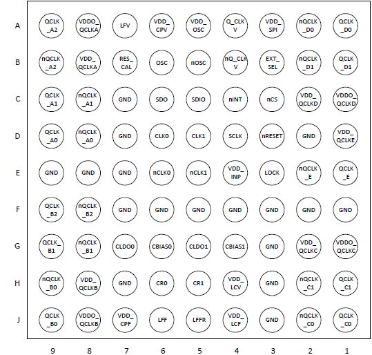
- Package: 81-FPBGA (8 × 8 mm, 0.8mm ball pitch)
- Temperature range: -40°C to +85°C
产品对比
应用
文档
相关文档
请登录后开启订阅
|
|
|
|
|---|---|---|
| 类型 | 文档标题 | 日期 |
| 数据手册 | PDF 1.22 MB | |
| 应用笔记 | PDF 91 KB | |
| 应用笔记 | PDF 1.99 MB | |
| 概览 | PDF 331 KB | |
| 应用笔记 | PDF 495 KB | |
| 应用笔记 | PDF 115 KB | |
| 应用笔记 | PDF 233 KB | |
| 应用笔记 | PDF 565 KB | |
| 应用笔记 | PDF 438 KB | |
9 items
|
||
设计和开发
模型
ECAD 模块
点击产品选项表中的产品,查找 SamacSys 中的原理图符号、PCB 足迹和 3D CAD 模型。点击产品选项表中的产品,查找 SamacSys 中的原理图符号、PCB 足迹和 3D CAD 模型。

产品选项
当前筛选条件
视频和培训
新闻和博客
| Benefits of a Point-of-Use Clock for Jitter Optimization | 博客 | 2021年4月27日 |