概览
描述
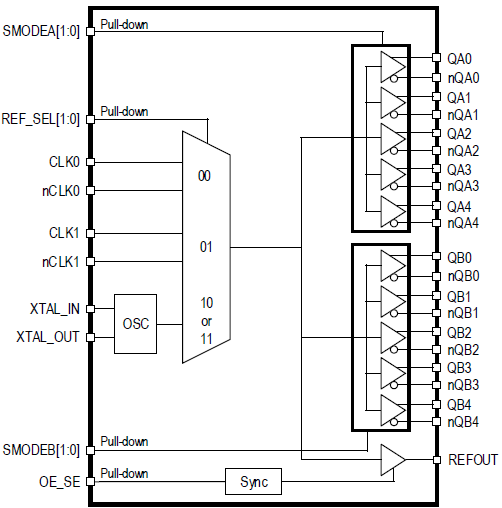
The 8T39210 is a high-performance clock fanout buffer. The input clock can be selected from two differential inputs or one crystal input. The internal oscillator circuit is automatically disabled if the crystal input is not selected. The crystal pin can be driven by a single-ended clock. The selected signal is distributed to ten differential outputs that can be configured as LVPECL, LVDS, or HSCL outputs. In addition, an LVCMOS output is provided. All outputs can be disabled into a high-impedance state. The device is designed for a signal fanout of high-frequency, low phase-noise clock and data signal. The outputs are at a defined level when inputs are open or tied to ground. It is designed to operate from a 3.3V or 2.5V core power supply, and either a 3.3V or 2.5V output operating supply.
特性
- Two differential reference clock input pairs
- Differential input pairs can accept the following differential input levels: LVPECL, LVDS, HCSL, HSTL, or single-ended
- Crystal input accepts 10MHz to 40MHz crystal or single-ended clock
- Maximum Output Frequency:
- LVPECL – 1.5GHz
- LVDS – 1.5GHz
- HCSL – 250MHz
- LVCMOS – 250MHz
- Two banks, each has five differential output pairs that can be configured as LVPECL, LVDS, or HCSL
- One single-ended reference output with synchronous enable to avoid clock glitch
- Output skew: 81ps (maximum), Bank A and Bank B at the same output level
- Part-to-part skew: 200ps (typical)
- Additive RMS phase jitter at 156.25MHz: 37.6fs RMS (12kHz–20MHz), typical at 3.3V/3.3V
- Supply voltage modes:
- VDD/VDDO
- 3.3V/3.3V
- 3.3V/2.5V
- 2.5V/2.5V
- -40 °C to 85 °C ambient operating temperature
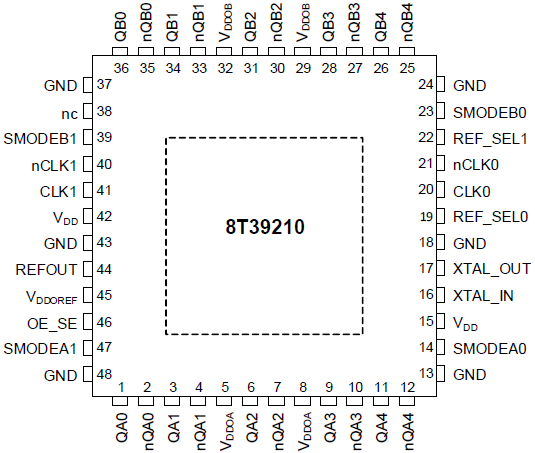
- 7mm × 7mm 48-VFQFPN lead-free (RoHS 6) packaging
产品对比
应用
设计和开发
模型
ECAD 模块
点击产品选项表中的产品,查找 SamacSys 中的原理图符号、PCB 足迹和 3D CAD 模型。点击产品选项表中的产品,查找 SamacSys 中的原理图符号、PCB 足迹和 3D CAD 模型。

产品选项
当前筛选条件
视频和培训
新闻和博客
| Buff Up Your Design with Renesas Clock Buffers | 博客 | 2018年12月15日 |