概览
描述
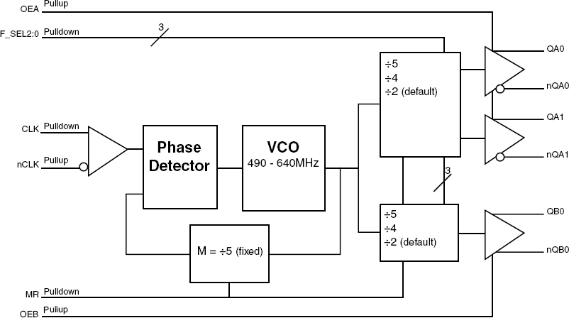
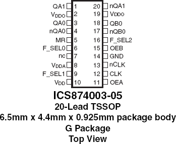
The 874003-05 is a high performance Differential-to-LVDS Jitter Attenuator designed for use in PCI Express® systems. In some PCI Express® systems, such as those found in desktop PCs, the PCI Express® clocks are generated from a low bandwidth, high phase noise PLL frequency synthesizer. In these systems, a jitter attenuator may be required to attenuate high frequency random and deterministic jitter components from the PLL synthesizer and from the system board. The 874003-05 has a bandwidth of 6.2MHz with <1dB peaking, easily meeting PCI Express® Gen2 PLL requirements. The 874003-05 uses IDT's 3rd Generation FemtoClock® PLL technology to achieve the lowest possible phase noise. The device is packaged in a 20 Lead TSSOP package, making it ideal for use in space constrained applications such as PCI Express® add-in cards.
特性
- Three differential LVDS output pairs
- One differential clock input
- CLK/nCLK can accept the following differential input levels: LVPECL, LVDS, LVHSTL, HCSL, SSTL
- Input frequency range: 98MHz to 128MHz
- Output frequency range: 98MHz to 320MHz
- VCO range: 490MHz - 640MHz
- Supports PCI Express® Spread-Spectrum Clocking
- High PLL bandwidth allows for better input tracking
- PCI Express® (2.5 Gb/s) and Gen 2 (5 Gb/S) jitter compliant
- 0°C to 70°C ambient operating temperature
- Full 3.3V operating supply
- Available in lead-free (RoHS 6) packages
产品对比
应用
设计和开发

产品选项
当前筛选条件
视频和培训
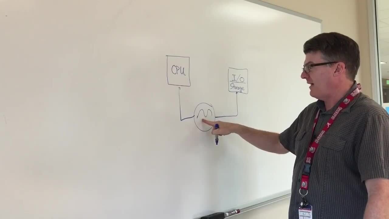
PCIe Clocking Architectures (Common and Separate)
This is the first video in our PCIe series. In this video, we define PCIe architectures, focusing on common and separate clock architectures. Watch the rest of the video series below where Ron will cover the impact of different timing architectures.
Watch the Video Series Below
Video List