概览
描述
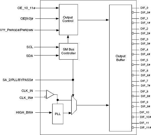
The CV128 differential buffer complies with Intel DB1200G rev. 0.5, and is designed to work in conjunction with the main clock of CK409, CK410/CK410M and CK410B etc., PLL is off in bypass mode and no clock detect.
特性
- Compliant with Intel DB1200G rev. 0.5
- DIF Clock Support ? 12differential clock output pairs @ 0.7 V ? 50 ps skew performance (same gear)
- OE pin Control of All Outputs
- 3.3 V Operation
- Gear Ratio supporting generation of clocks at a different frequency ratioed from the input.
- Split outputs supporting options of 2 outputs @1:1 and remaining 10 pairs at an alternate gear
- Pin level OE control of individual outputs
- Multiple output frequency options up to 400Mhz as a gear ratio of input clocks of 100-400Mhz
- Output is HCSL compatible
- SMBus Programmable configurations
- PLL Bypass Configurable
- SMBus address configurable to allow multiple buffer control in a single control network
- Programmable Bandwidth
- Glitchfree transition between frequency states
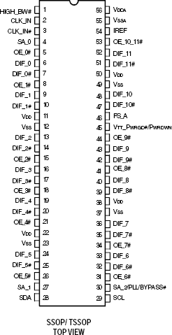
- Available in SSOP and TSSOP packages
产品对比
应用
设计和开发
模型
ECAD 模块
点击产品选项表中的 CAD 模型链接,查找 SamacSys 中的原理图符号、PCB 焊盘布局和 3D CAD 模型。如果符号和模型不可用,可直接在 SamacSys 请求该符号或模型。

产品选项
当前筛选条件