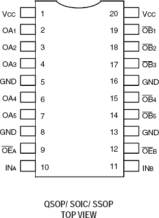
| Lead Count (#) | 20 |
| Pkg. Type | SOIC |
| Pkg. Code | PSG20 |
| Pitch (mm) | 1.27 |
| Pkg. Dimensions (mm) | 12.8 x 7.6 x 2.34 |
| Pb (Lead) Free | Yes |
| ECCN (US) | EAR99 |
| HTS (US) | 8542390000 |
| Moisture Sensitivity Level (MSL) | 1 |
| Pkg. Type | SOIC |
| Lead Count (#) | 20 |
| Pb (Lead) Free | Yes |
| Carrier Type | Tube |
| Core Voltage (V) | 5 |
| Function | Buffer |
| Input Type | LVCMOS |
| Inputs (#) | 2 |
| Length (mm) | 12.8 |
| MOQ | 222 |
| Moisture Sensitivity Level (MSL) | 1 |
| Output Banks (#) | 2 |
| Output Skew (ps) | 500 |
| Output Type | LVCMOS |
| Output Voltage (V) | 5 |
| Outputs (#) | 10 |
| Package Area (mm²) | 97.3 |
| Pb Free Category | e3 Sn |
| Pitch (mm) | 1.27 |
| Pkg. Dimensions (mm) | 12.8 x 7.6 x 2.34 |
| Qty. per Carrier (#) | 37 |
| Qty. per Reel (#) | 0 |
| Requires Terms and Conditions | Does not require acceptance of Terms and Conditions |
| Tape & Reel | No |
| Temp. Range | 0 to 70°C |
| Thickness (mm) | 2.34 |
| Width (mm) | 7.6 |
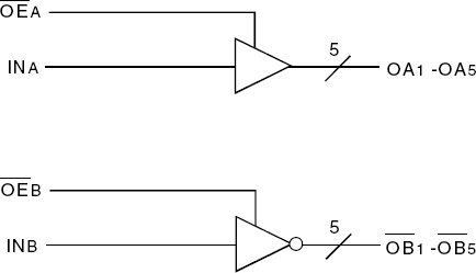
The 74FCT810T is a dual bank inverting/non-inverting clock driver built using advanced dual metal CMOS technology. It consists of two banks of drivers, one inverting and one non-inverting. Each bank drives five output buffers from a standard TTL-compatible input. The FCT810T has a low output skew, pulse skew, and package skew. Inputs are designed with hysteresis circuitry for improved noise immunity. The outputs are designed with TTL output levels and controlled edge rates to reduce signal noise. The part has multiple grounds, minimizing the effects of ground inductance.