封装信息
| CAD 模型: | View CAD Model |
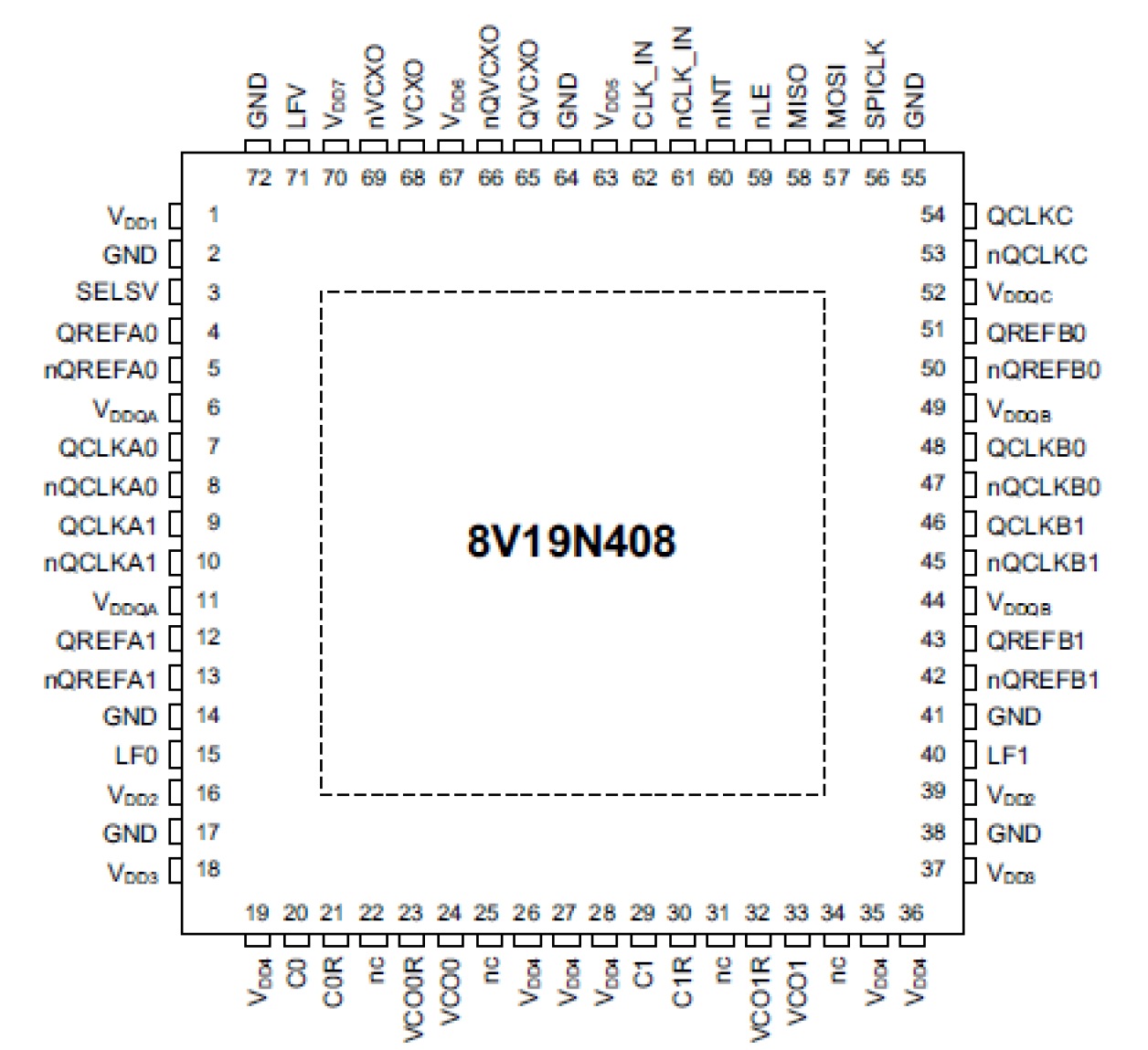
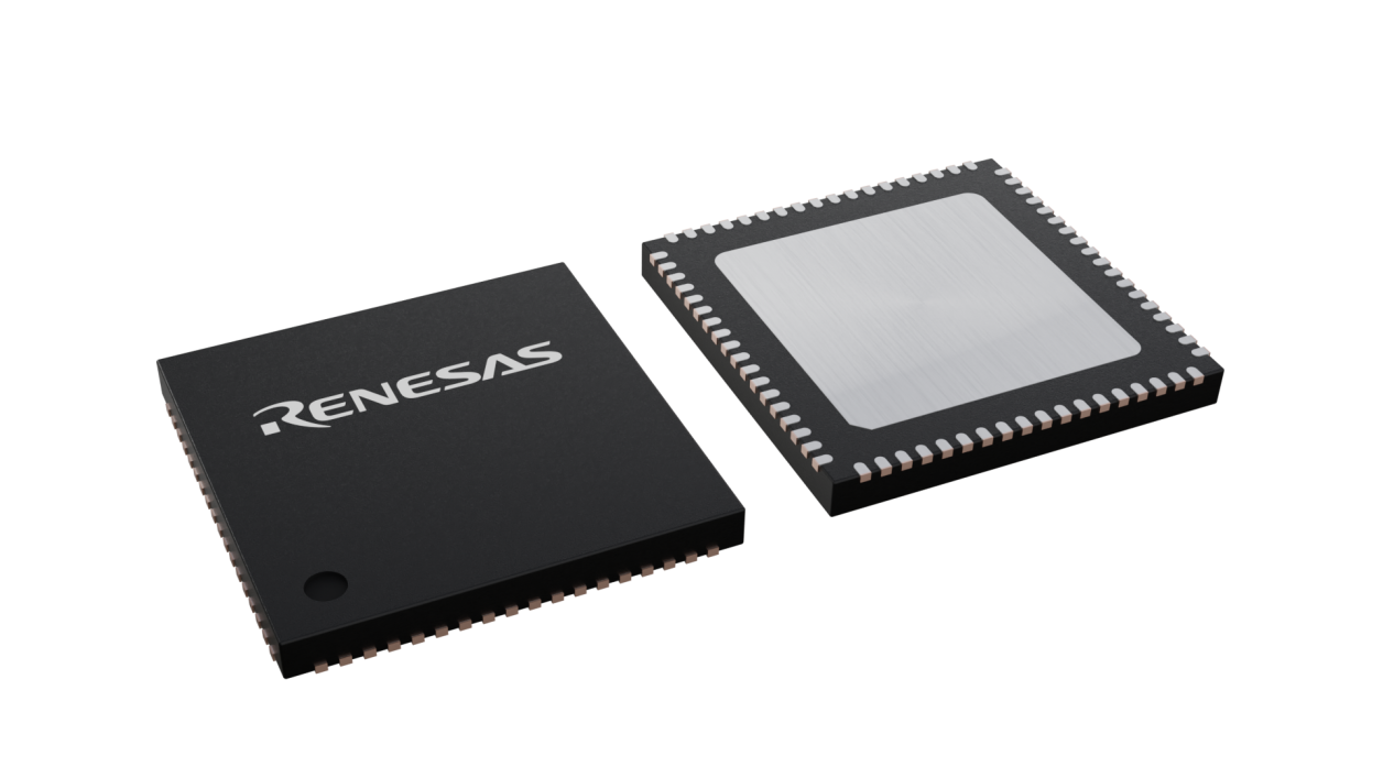
| Pkg. Type: | VFQFPN |
| Pkg. Code: | NLG72 |
| Lead Count (#): | 72 |
| Pkg. Dimensions (mm): | 10.0 x 10.0 x 1.0 |
| Pitch (mm): | 0.5 |
环境和出口类别
| Moisture Sensitivity Level (MSL) | 3 |
| Pb (Lead) Free | Yes |
| ECCN (US) | EAR99 |
| HTS (US) | 8542.39.0090 |
产品属性
| Lead Count (#) | 72 |
| Carrier Type | Tray |
| Moisture Sensitivity Level (MSL) | 3 |
| Qty. per Reel (#) | 0 |
| Qty. per Carrier (#) | 168 |
| Pb (Lead) Free | Yes |
| Pb Free Category | e3 Sn |
| Temp. Range (°C) | -40 to 85°C |
| Adjustable Phase | Yes |
| Advanced Features | JESD204B, Holdover, Phase Delay, Programmable Clock |
| Core Voltage (V) | 3.3 |
| Feedback Divider Resolution (bits) | 15 |
| Fractional Output Dividers (#) | 0 |
| Frequency Plan | 2457.6 / Output_Divider, 2500 / Output_Divider, 2949.12 / Output_Divider |
| Input Freq (MHz) | 0.01 - 250 |
| Input Redundancy | Clock Monitor, Holdover |
| Input Ref. Divider Resolution (bits) | 8 |
| Input Type | LVPECL, LVDS |
| Inputs (#) | 1 |
| JESD204B/C Compliant | Yes |
| Length (mm) | 10 |
| Loop Bandwidth Range (Hz) | 30 - 30 |
| MOQ | 168 |
| Noise Floor (dBc/Hz) | -160 |
| Output Banks (#) | 3 |
| Output Divider Resolution (bits) | 5 |
| Output Freq Range (MHz) | 25 - 2949.12 |
| Output Skew (ps) | 65 |
| Output Type | LVDS, LVPECL |
| Output Voltage (V) | 3.3 |
| Outputs (#) | 10 |
| Package Area (mm²) | 100 |
| Phase Jitter Typ RMS (fs) | 80.4 |
| Phase Jitter Typ RMS (ps) | 0.08 |
| Phase Noise Supports GSM | Yes |
| Pitch (mm) | 0.5 |
| Pkg. Dimensions (mm) | 10.0 x 10.0 x 1.0 |
| Pkg. Type | VFQFPN |
| Product Category | JESD204B/C, Jitter Attenuators |
| Prog. Clock | Yes |
| Requires Terms and Conditions | Does not require acceptance of Terms and Conditions |
| Supply Voltage (V) | 3.3 - 3.3 |
| Synthesis Mode | Integer |
| Tape & Reel | No |
| Thickness (mm) | 1 |
| Width (mm) | 10 |
| Xtal Freq (KHz) | 25 - 250 |
有关 8V19N408 的资源
描述
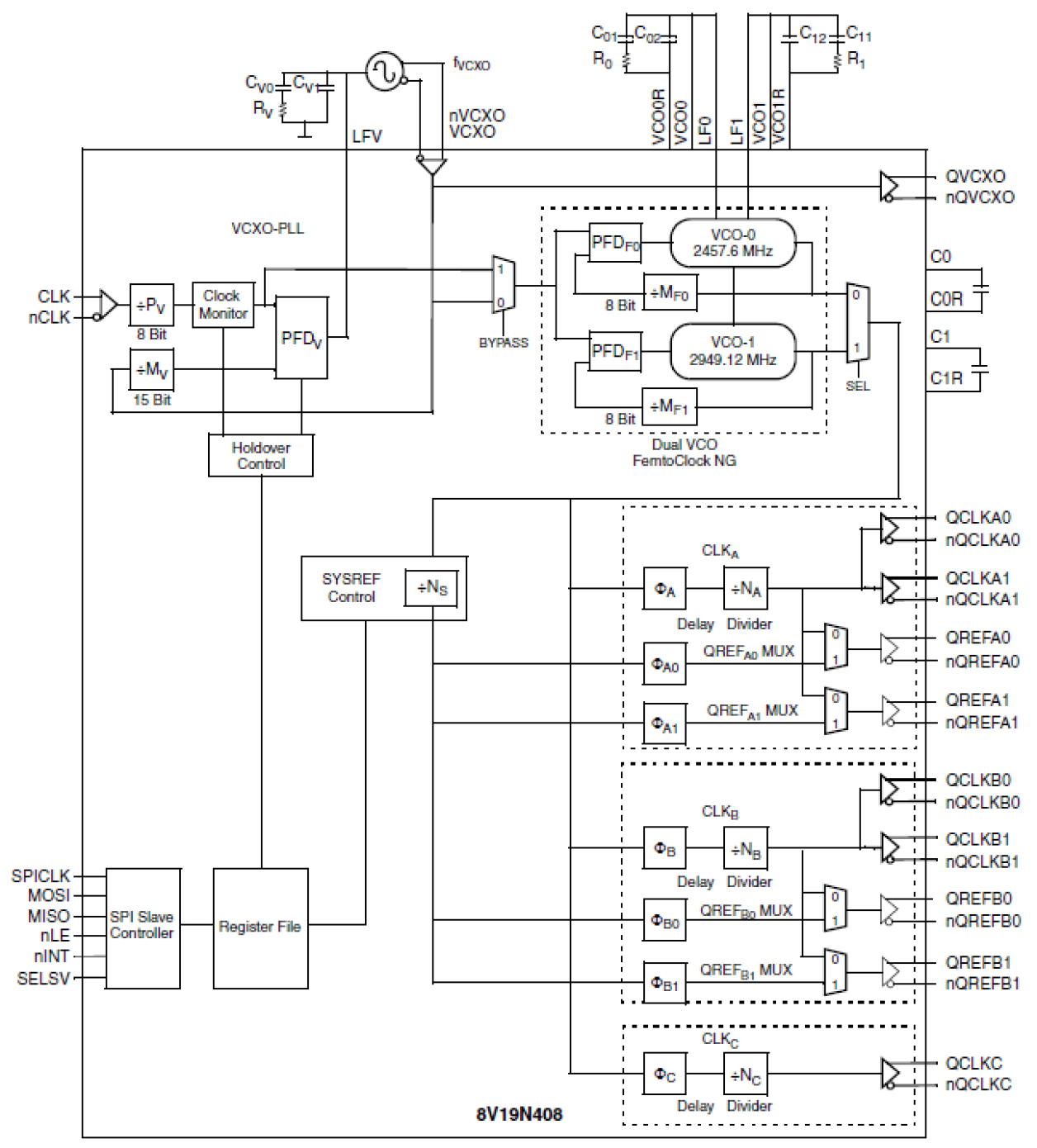
The 8V19N408 is a fully integrated FemtoClock® NG jitter attenuator and clock synthesizer. The device is a high-performance clock solution for conditioning and frequency/phase management of wireless base station radio equipment boards and is optimized to deliver excellent phase noise performance. The device supports JESD204B subclass 0 and 1 clock implementations. The device is very flexible in programming the output frequency and phase. A two-stage PLL architecture supports both jitter attenuation and frequency multiplication. The first stage PLL is the jitter attenuator and uses an external VCXO for best possible phase noise characteristics. The second stage PLL lock on the VCXO-PLL output signal and synthesizes the target frequency. For flexibility, the second-stage PLL can use one of two VCOs at 2400MHz - 2500MHz (VCO-0) and 2920MHz - 3000MHz (VCO-1).
The device supports the clock generation of high-frequency clocks from the selected VCO and low-frequency system reference signals (SYSREF). The system reference signals are internally synchronized to the clock signals. Delay functions exist for achieving alignment and controlled phase delay between system reference and clock signals and to align/delay individual output signals. The input is monitored for activity. Short-term hold-over is provided to handle clock input failure scenarios. Auto-lock, individually programmable output frequency dividers, and phase adjustment capabilities are added for flexibility. The device is configured through a 4-wire SP serial interface and reports lock and signal loss status in internal registers and optionally via lock detect (nINT) output. The device is packaged in a lead-free (RoHS 6) 72-lead VFQFN package. The extended temperature range supports wireless infrastructure, telecommunication, and networking end equipment requirements.


