概览
描述
The 9DB401 follows the Intel DB400 Differential Buffer Specification v2.0. This buffer provides four PCI-Express SRC clocks. The 9DB401 is driven by a differential input pair from a CK409/CK410/CK410M main clock generator, such as the 952601, 954101 or 954201. It provides outputs meeting tight cycle-to-cycle jitter (50 ps) and output-to-output skew (50ps) requirements.
特性
- 4- 0.7 V HCSL differential output pairs
- Phase jitter: PCIe Gen1 < 86 ps peak to peak
- Supports zero delay buffer mode and fanout mode
- Bandwidth programming available
- 50-100 MHz operation in PLL mode
- 50-400 MHz operation in Bypass mode
产品对比
应用
设计和开发

产品选项
当前筛选条件
视频和培训
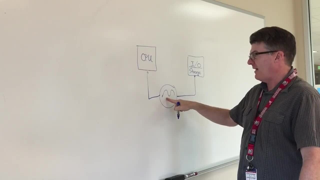
PCIe Clocking Architectures (Common and Separate)
This is the first video in our PCIe series. In this video, we define PCIe architectures, focusing on common and separate clock architectures. Watch the rest of the video series below where Ron will cover the impact of different timing architectures.
Watch the Video Series Below
Video List