概览
描述
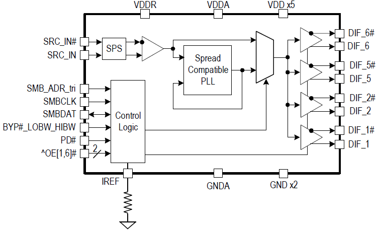
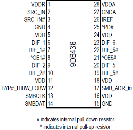
The 9DB436 is a zero delay/fanout buffer for PCI Express™ clocking. It supports PCIe Gen 1–3 in zero delay mode and PCIe Gen 1–4 in fanout mode. The 9DB436 also features a Safe Power Sequence (SPS) clock input. The 9DB436 is a pin-compatible upgrade to the 9DB433 and 9DB434.
特性
- Four 0.7V current-mode differential HCSL output pairs
- PCIe Gen 3 jitter < 0.6ps RMS in ZDB mode
- PCIe Gen 4 additive jitter < 0.1ps RMS in fanout mode
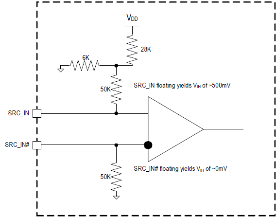
- SPS internal receiver bias network keeps the input clock parked when input is floating
- Supports both 85Ω and 100Ω output impedance with appropriate resistor selection
- OE# pins default to controlling outputs
- Supports zero delay buffer mode and fanout mode
- Selectable PLL bandwidth; minimizes jitter peaking in downstream PLLs
- Spread spectrum compatible
- Three selectable SMBus addresses
产品对比
应用
设计和开发

产品选项
当前筛选条件
视频和培训
PCIe Clocking Architectures (Common and Separate)
This is the first video in our PCIe series. In this video, we define PCIe architectures, focusing on common and separate clock architectures. Watch the rest of the video series below where Ron will cover the impact of different timing architectures.
Watch the Video Series Below
Video List