概览
描述
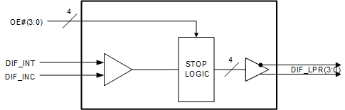
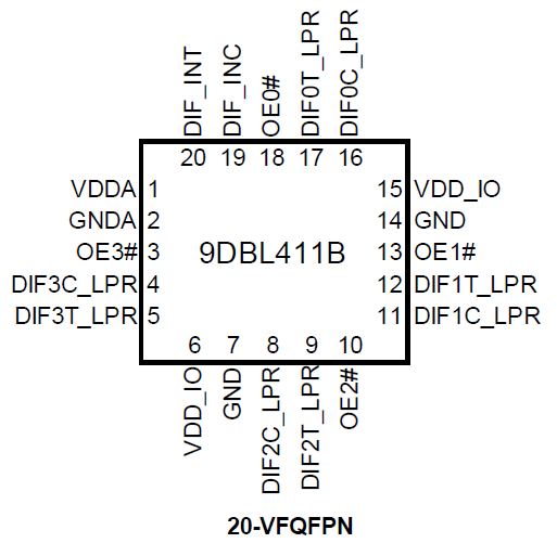
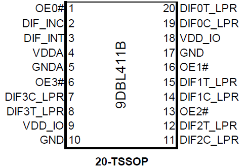
The 9DBL411 is a four-output lower power differential buffer. Each output has its own OE# pin. The device has a maximum operating frequency of 150MHz.
特性
- Four low-power differential output pairs
- Individual OE# control of each output pair
- Output cycle-cycle jitter < 25ps additive
- Output-to-output skew: < 50ps
- Low-power differential fanout buffer for PCI Express and CPU clocks
- Available in commercial (0 °C to +70 °C) and industrial (-40 °C to +85 °C) temperature ranges
- Available in 20-VFQFPN or 20-TSSOP packages
产品对比
应用
设计和开发

产品选项
当前筛选条件
视频和培训
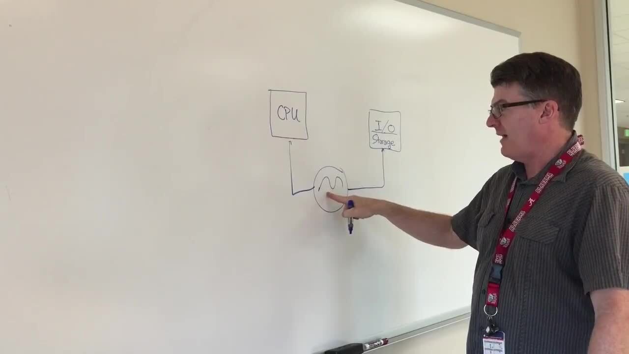
PCIe Clocking Architectures (Common and Separate)
This is the first video in our PCIe series. In this video, we define PCIe architectures, focusing on common and separate clock architectures. Watch the rest of the video series below where Ron will cover the impact of different timing architectures.
Watch the Video Series Below
Video List