概览
描述
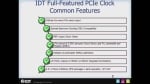
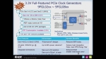
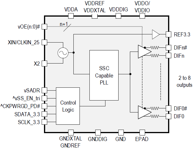
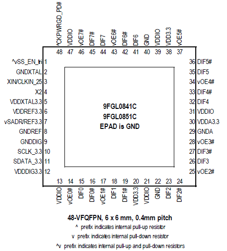
The 9FGL0841/51 devices are 8-output 3.3V PCIe Gen 1–6 clock generators. Each output has a dedicated OE# pin supporting PCIe CLKREQ# functionality. Two different spread spectrum levels, in addition to spread off, are supported. The 9FGL0841/51 supports PCIe Gen 1–6 Common Clocked architectures (CC), PCIe Separate Reference no Spread (SRNS), and Separate Reference Independent Spread (SRIS) clocking architectures.
For information regarding evaluation boards and material, please contact your local sales representative.
特性
- PCIe Gen 1–6 CC-compliant
- Supports PCIe SRIS and SRNS clocking
- Integrated terminations for 100Ω and 85Ω systems save 4 resistors per output
- Pin-selectable SRNS 0%, CC 0%, and CC/SRIS -0.5% spread
- SMBus-selectable CC/SRIS -0.25% spread
- One 3.3V LVCMOS REF output with Wake-On-LAN (WOL) support
- Easy AC coupling to other logic families, see application note AN-891.
- Space-saving 6mm × 6mm 48-VFQFPN
产品对比
应用
设计和开发
软件与工具
开发板与套件
评估
EVK9FGL0841
有效
Evaluation Board for the 100ohm 9FGL0841 PCIe Clock Generator
This is the evaluation board for the 9FGL0841 clock generator.
Recommended Documents:
模型
ECAD 模块
点击产品选项表中的 CAD 模型链接,查找 SamacSys 中的原理图符号、PCB 焊盘布局和 3D CAD 模型。如果符号和模型不可用,可直接在 SamacSys 请求该符号或模型。

产品选项
当前筛选条件
视频和培训
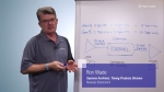
PCIe Reference Clock Jitter Budgets
Ron Wade, chief PCIe system architect explains the fundamental difference in reference clock jitter budgets between the first three generations of the specification and those of Gen4 and Gen5 which raise new challenges for designers.
Related Resources
Video List