概览
描述
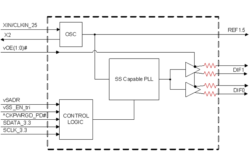
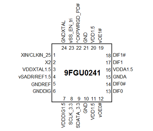
The 9FGU0241 is a member of IDT's 1.5 V Ultra-Low-Power PCIe clock family with integrated output terminations providing Zo=100 Ω. The device has 2 output enables for clock management, 2 different spread spectrum levels in addition to spread off, and 2 selectable SMBus addresses.
特性
- Direct connection to 100ohm transmission lines; saves 16 resistors compared to standard PCIe devices
- 23 mW typical power consumption; reduced thermal concerns
- OE# pins; support DIF power management
- Programmable slew rate for each output; allows tuning for various line lengths
- Programmable output amplitude; allows tuning for various application environments
- DIF outputs blocked until PLL is locked; clean system start-up
- Selectable 0%, -0.25% or -0.5% spread on DIF outputs; reduces EMI
- External 25 MHz crystal; supports tight ppm with 0 ppm synthesis error
- Configuration can be accomplished with strapping pins; SMBus interface not required for device control
- 3.3 V tolerant SMBus interface works with legacy controllers
- Space saving 4x4mm 24-pin VFQFPN; minimal board space
- Selectable SMBus addresses; multiple devices can easily share an SMBus segment
产品对比
应用
设计和开发
模型
ECAD 模块
点击产品选项表中的 CAD 模型链接,查找 SamacSys 中的原理图符号、PCB 焊盘布局和 3D CAD 模型。如果符号和模型不可用,可直接在 SamacSys 请求该符号或模型。

产品选项
当前筛选条件
支持


视频和培训
This is the first video in our PCIe series. In this video, we define PCIe architectures, focusing on common and separate clock architectures. Watch the rest of the video series below where Ron will cover the impact of different timing architectures.
Watch the Video Series Below