概览
描述
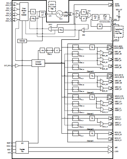
The 8V19N491-36 is a fully integrated FemtoClock™ NG jitter attenuator and clock synthesizer. The device is designed as a high-performance clock solution for conditioning and frequency/phase management of wireless base station radio equipment boards. The device is optimized to deliver excellent phase noise performance as required in GSM, WCDMA, LTE, and LTE-A radio board implementations. The device supports JESD204B subclass 0 and 1 clocks. A two-stage PLL architecture supports both jitter attenuation and frequency multiplication. The first stage PLL is the jitter attenuator and uses an external VCXO for best possible phase noise characteristics. The second stage PLL locks on the VCXO-PLL output signal and synthesizes the target frequency.
The 8V19N491-36 supports the clock generation of high-frequency clocks from the selected VCO and low-frequency synchronization signals (SYSREF). SYSREF signals are internally synchronized to the clock signals. Delay functions exist for achieving alignment and controlled phase delay between system reference and clock signals and to align/delay individual output signals. The four redundant inputs are monitored for activity. Four selectable clock switching modes are provided to handle clock input failure scenarios. Auto-lock, individually programmable output frequency dividers, and phase adjustment capabilities are added for flexibility. The device is configured through a 3/4-wire SPI interface and reports lock and signal loss status in internal registers and via a lock detect (LOCK) output. Internal status bit changes can also be reported via the nINT output. The 8V19N491-36 is ideal for driving converter circuits in wireless infrastructure, radar/imaging, and instrumentation/medical applications.
For information regarding evaluation boards and material, contact your local sales representative.
特性
- High-performance clock RF-PLL with support for JESD204B
- Optimized for low phase noise: -152.5dBc/Hz (800kHz offset; 245.76MHz clock)
- Integrated phase noise of 65fs RMS typical (12kHz to 20MHz) at 737.28MHz
- Dual-PLL architecture
- First PLL stage with external VCXO for clock jitter attenuation
- Second PLL with internal FemtoClock NG PLL: 3686.4MHz
- For 3932.16MHz: see 8V19N492-39
- For 2949.12MHz: see 8V19N492 and 8V19N490A
- For 2457.6MHz: see 8V19N490-24 and 8V19N491-24
- For 1966.08MHz: see 8V19N490-19
- Five output channels with a total of 18 outputs
- Configurable integer clock frequency dividers
- Supported clock output frequencies include: 3686.4, 1843.2, 1228.8, 737.28, 614.4, 368.4, 307.2, 245.76, 153.6, 122.88, and 61.44 MHz
- Low-power LVPECL/LVDS outputs support configurable signal amplitude
- Phase delay circuits
- Redundant input clock architecture with four inputs including input activity monitoring and switching
- SYSREF generation modes include internal and external trigger mode for JESD204B
- Supply voltage: 3.3V
- SPI Interface, 3/4 wire configurable
- Package: 11mm x 11mm, 100-CABGA
- Temperature range: -40 °C to +85 °C
产品对比
应用
设计和开发

产品选项
当前筛选条件
视频和培训
新闻和博客
博客
2021年4月27日
|