概览
描述
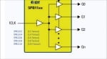
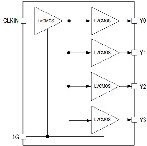
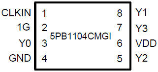
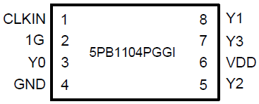
The 5PB1104 is a high-performance 1:4 LVCMOS clock buffer that offers a best-in-class additive phase jitter of 50fs RMS. This clock buffer also supports an Output Enable function. It is available in 8-pin DFN and TSSOP packages and can operate from a 1.8V to 3.3V supply.
特性
- High-performance 1:4 LVCMOS clock buffer
- Very low pin-to-pin skew: < 50ps
- Very low additive jitter: < 50fs
- Supply voltage: 1.8V to 3.3V
- fMAX = 200MHz
- Integrated serial termination for 50Ω channel
- Packaged in 8-pin TSSOP and small DFN packages
- Extended (-40 °C to +105 °C) temperature range
- AEC-Q100 qualified, Automotive Grade 1 (-40 °C to +125 °C)
产品对比
应用
设计和开发

产品选项
当前筛选条件
视频和培训
5PB11xx Ultra Low Jitter LVCMOS Buffers
This video provides an overview of the LVCMOS High Performance Clock Buffer Family, highlighting their key features and capabilities.
Related Resources

Video List