概览
描述
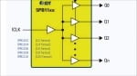
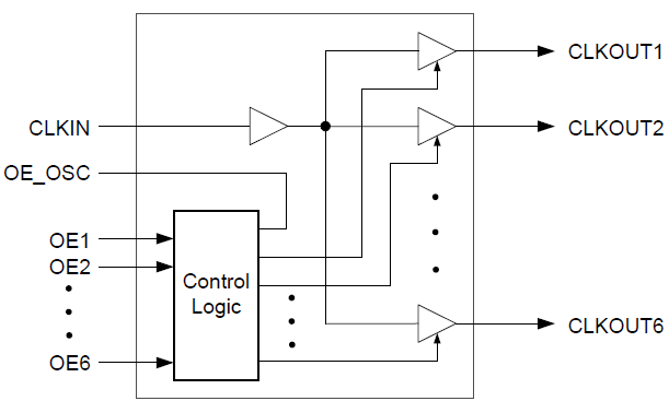
The 5PB1204 is a high-performance TCXO/LVCMOS clock fanout buffer with individual OE pins for each output. The CLKIN pin can accept either a square wave (LVCMOS) or a clipped sine wave (such as TCXO clipped sine wave output) as input.
The 5PB1204 has industry-leading low jitter and extremely low current consumption, making it ideal for smart mobile devices.
特性
- Extremely low operating and standby current consumption
- Low RMS Additive Phase jitter
- 1.8V power supply voltage
- Four outputs with individual Output Enable pin
- One input
- OE_OSC control pin to enable/disable reference TCXO / XO
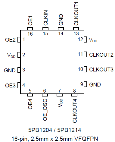
- Small 16-pin VFQFPN package
- Extended temperature range (-40 °C to +105 °C)
产品对比
应用
文档
相关文档
请登录后开启订阅
|
|
|
|
|---|---|---|
| 类型 | 文档标题 | 日期 |
| 数据手册 | PDF 292 KB | |
| 应用说明 | PDF 187 KB | |
| 概览 | PDF 217 KB | |
| 产品变更通告 | PDF 268 KB | |
| 概览 | PDF 252 KB | |
| 应用说明 | PDF 495 KB | |
| 应用说明 | PDF 442 KB | |
| 应用说明 | PDF 565 KB | |
8 items
|
||
设计和开发

产品选项
当前筛选条件
视频和培训
5PB11xx Ultra Low Jitter LVCMOS Buffers
This video provides an overview of the LVCMOS High Performance Clock Buffer Family, highlighting their key features and capabilities.
Related Resources

Video List