概览
描述
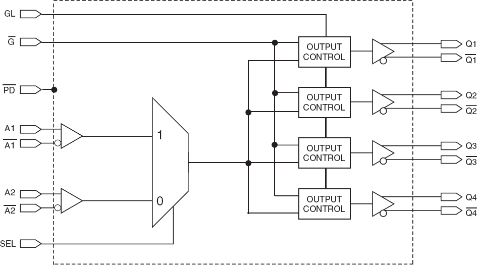
The 5T9304I differential clock buffer is a user-selectable differential input to four LVDS outputs. The fanout from a differential input to four LVDS outputs reduces loading on the preceding driver and provides an efficient clock distribution network. The 5T9304I can act as a translator from a differential HSTL, eHSTL, LVEPECL (2.5V), LVPECL (3.3V), CML, or LVDS input to LVDS outputs. A single-ended 3.3V / 2.5V LVTTL input can also be used to translate to LVDS outputs. The redundant input capability allows for an asynchronous change-over from a primary clock source to a secondary clock source. Selectable reference inputs are controlled by SEL. The 5T9304I outputs can be asynchronously enabled/disabled. When disabled, the outputs will drive to the value selected by the GL pin. Multiple power and grounds reduce noise.
特性
- Guaranteed low skew: 50ps (maximum)
- Very low duty cycle distortion: 125ps (maximum)
- Propagation delay: 1.75ns (maximum)
- Up to 450MHz operation
- Selectable inputs
- Hot insertable and over-voltage tolerant inputs
- 3.3V/2.5V LVTTL, HSTL eHSTL, LVEPECL (2.5V), LVPECL (3.3V), CML or LVDS input interface
- Selectable differential inputs to four LVDS outputs
- 2.5V VDD
- -40°C to 85°C ambient operating temperature
- Available in lead-free (RoHS 6) package
产品对比
应用
设计和开发
模型
ECAD 模块
点击产品选项表中的 CAD 模型链接,查找 SamacSys 中的原理图符号、PCB 焊盘布局和 3D CAD 模型。如果符号和模型不可用,可直接在 SamacSys 请求该符号或模型。

产品选项
当前筛选条件