概览
描述
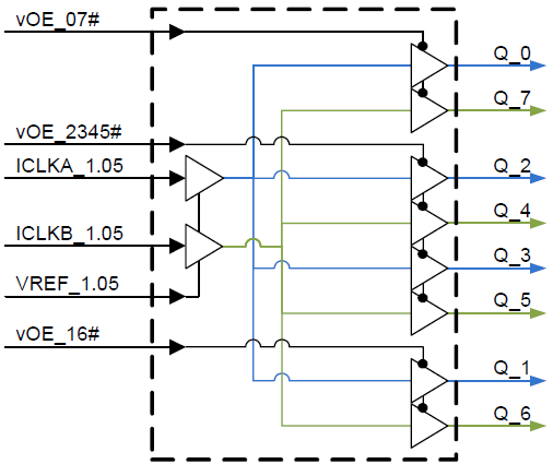
The 9SBV0802 provides two banks of four 1.05V LVCMOS outputs. Each bank has its own input. There are three OE pins. Two OE pins control two outputs each and one OE pin controls four outputs. One 9SBV0802 allows one PCH to easily support four CPUs with point-to-point routing of the PM signals. Two 9SBV0802 devices allow one PCH to easily support up to eight CPUs with point-to-point routing of the PM signals.
特性
- Eight 1MHz – 48MHz 1.05V LVCMOS outputs
- Additive cycle-to-cycle jitter < 8ps
- Output-to-output skew within a bank < 50ps
- Output-to-output skew between banks < 100ps
- 1.8V power supply, 15mW typical power consumption
- Three OE pins
- 1.05V LVCMOS inputs with VREF pin
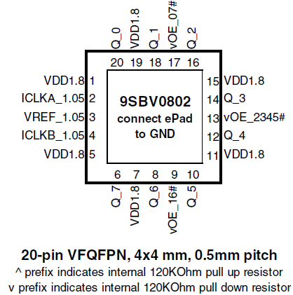
- Space saving 4mm x 4mm 20-VFQFPN
产品对比
应用
设计和开发

产品选项
当前筛选条件
视频和培训
Low-jitter LVCMOS Fanout Clock Buffers by IDT
This video overviews the LVCMOS Fanout Buffers, showcasing their best-in-class performance with extremely low phase jitter, minimal output skew, and low power consumption, along with other competitive features.
Video List