封装信息
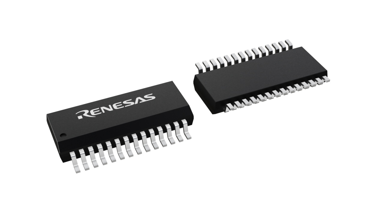
| CAD 模型: | View CAD Model |
| Pkg. Type: | QSOP |
| Pkg. Code: | MLE |
| Lead Count (#): | 28 |
| Pkg. Dimensions (mm): | 9.9 x 3.9 x 1.55 |
| Pitch (mm): | 0.6 |
环境和出口类别
| ECCN (US) | EAR99 |
| HTS (US) | 8542.39.0090 |
| RoHS (ISL6539CAZ-T) | 下载 |
| Moisture Sensitivity Level (MSL) | 3 |
| Pb (Lead) Free | Yes |
产品属性
| Pkg. Type | QSOP |
| Carrier Type | Reel |
| Bias Voltage Range (V) | 6.5 - 6.5 |
| DDR Capable | Yes |
| Input Voltage (Max) (V) | 18 |
| Input Voltage (Min) (V) | 3.3 |
| Lead Count (#) | 28 |
| Length (mm) | 9.9 |
| Linear Output | No |
| MOQ | 2500 |
| Moisture Sensitivity Level (MSL) | 3 |
| Output Current 1 (Max) (A) | 8 |
| Output Voltage (Min) (V) | 0.9 |
| Output Voltage 1 (Max) (V) | 5.5 |
| Outputs (#) | 2 |
| Pb (Lead) Free | Yes |
| Pb Free Category | Pb-Free 100% Matte Tin Plate w/Anneal-e3 |
| Pitch (mm) | 0.6 |
| Pkg. Dimensions (mm) | 9.9 x 3.9 x 1.55 |
| Qualification Level | Standard |
| Switching Frequency Range (Typical) (kHz) | 300 - 300 |
| Temp. Range (°C) | 0 to +70°C |
| Thickness (mm) | 1.55 |
| Width (mm) | 3.9 |
有关 ISL6539 的资源
描述
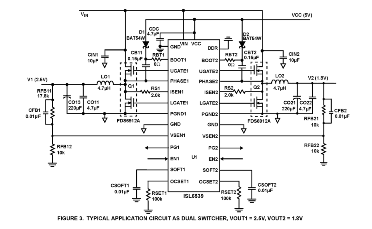
The ISL6539 dual PWM controller delivers high efficiency and tight regulation from two voltage regulating synchronous buck DC/DC converters. It was designed especially for DDR DRAM, SDRAM, graphic chipset applications, and system regulators in high performance applications. Voltage-feed-forward ramp modulation, current mode control, and internal feedback compensation provide fast response to input voltage and output load transients. Input current ripple is minimized by channel-to-channel PWM phase shift of 0°, 90° or 180° (determined by input voltage and status of the DDR pin). The ISL6539 can control two independent output voltages adjustable from 0.9V to 5.5V or, by activating the DDR pin, transform into a complete DDR memory power supply solution. In DDR mode, CH2 output voltage VTT tracks CH1 output voltage VDDQ. CH2 output can both source and sink current, an essential power supply feature for DDR memory. The reference voltage VREF required by DDR memory is generated as well. In dual power supply applications the ISL6539 monitors the output voltage of both CH1 and CH2. An independent PGOOD (power good) signal is asserted for each channel after the soft-start sequence has completed, and the output voltage is within PGOOD window. In DDR mode CH1 generates the only PGOOD signal. Built-in overvoltage protection prevents the output from going above 115% of the set point by holding the lower MOSFET on and the upper MOSFET off. When the output voltage decays below the overvoltage threshold, normal operation automatically resumes. Once the soft-start sequence has completed, undervoltage protection latches the offending channel off if the output drops below 75% of its set point value for the dual switcher. Adjustable overcurrent protection (OCP) monitors the voltage drop across the rDS(ON) of the lower MOSFET. If more precise current-sensing is required, an external current sense resistor may be used.

