| Lead Count (#) | 16 |
| Pitch (mm) | 0.4 |
| Pkg. Type | STQFN-16 |
| Pkg. Dimensions (mm) | 1.6 x 2.5 mm |
| Moisture Sensitivity Level (MSL) | 1 |
| Pb (Lead) Free | Yes |
| ECCN (US) | |
| HTS (US) |
| Lead Count (#) | 16 |
| Carrier Type | Tape & Reel |
| Moisture Sensitivity Level (MSL) | 1 |
| Pb (Lead) Free | Yes |
| Temp. Range | -40 to +85°C |
| Country of Assembly | China, Taiwan |
| Country of Wafer Fabrication | Taiwan |
| Price (USD) | 0.73065 |
| Current Monitor Output | No |
| Discharge Circuit | Yes |
| Enable | Active High |
| FET Pass Device Type | Single N-Channel |
| IDS (A) | 5 |
| IDS Channel 1 (A) | 5 |
| Internal TVS Surge Protection | No |
| MOQ | 3000 |
| Output Discharge Circuit | Yes |
| Output Voltage Slew Rate set by | Capacitor |
| Over Current Protection (OCP) | Adjustable |
| Over Current Protection Setting Range Channel 1 | 2.1 - 6 |
| Over Temperature Protection (OTP) | Yes |
| Over Voltage Protection | No |
| Over Сurrent Protection Setting Range (A) | 2.1 - 6 |
| Parametric Category | Load Switches |
| Pitch (mm) | 0.4 |
| Pkg. Dimensions (mm) | 1.6 x 2.5 mm |
| Pkg. Type | STQFN-16 |
| Power Good (PG), FAULT indicator | PG |
| Power Monitor Output | No |
| Protection Features | CL (R), TSD |
| Qty. per Reel (#) | 3000 |
| RDSON (Typ) (mΩ) | 4 |
| RDSON (Typ) Channel 1 (mΩ) | 4 |
| Ramp Control | Capacitor |
| Reverse current blocking | No |
| Reverse voltage detection | No |
| Short Circuit Protection | Yes |
| Undervoltage Protection | Yes |
| VD/VIN (Max) | VDD |
| VD/VIN (Min) | 0.8 |
| VDD Range (V) (V) | 2.5 - 5.5 |
| VDD max. (V) | 5.5 |
| VDD min. (V) | 2.5 |
| VDDl-VDDh (V) | 2.5 - 5.5 |
| VIN Channel 1 max. (V) | 5.5 |
| VIN Channel 1 min. (V) | 0.8 |
| VIN Range (V) | 0.8 - 5.5 |
| VIN Range Channel 1 (V) | 0.8 - 5.5 |
| VIN max. (V) | 5.5 |
| VIN min. (V) | 0.8 |
| VOUT Discharge Circuit | Yes |
| 已发布 | Yes |
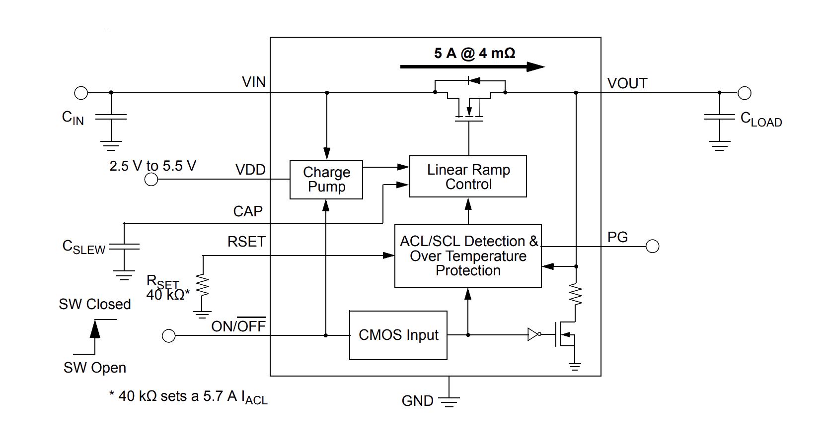
Operating from a 2.5V to 5.5V power supply and fully specified over the -40 °C to 85 °C industrial temperature range, the SLG59M1717V is a high‑performance 4mΩ, 5A single‑channel nFET load switch designed for all 0.8V to 5.5V power rail applications. The SLG59M1717V features adjustable inrush current control which is achieved by adjusting the VOUT slew rate with an external capacitor. Using a proprietary MOSFET design, the SLG59M1717V achieves a stable 4mΩ RDSON across a wide input/supply voltage range. The SLG59M1717V also incorporates resistor‑adjustable current limiting as well as thermal protection. Using proprietary technology for high‑current operation, the SLG59M1717V is packaged in a space‑efficient, low thermal resistance, RoHS‑compliant 1.6mm x 2.5mm STQFN package.