概览
描述
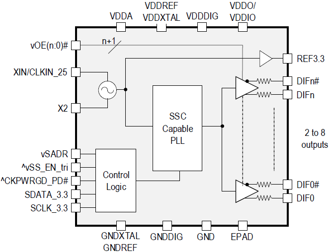
The 9FGL0441/51 devices are 4-output 3.3V PCIe Gen 1–6 clock generators. Each output has a dedicated OE# pin supporting PCIe CLKREQ# functionality. Two different spread spectrum levels, in addition to spread off, are supported. The 9FGL0441/51 supports PCIe Gen 1–6 Common Clocked architectures (CC), PCIe Separate Reference no Spread (SRNS), and Separate Reference Independent Spread (SRIS) clocking architectures.
特性
- PCIe Gen 1–6 CC-compliant
- Supports PCIe SRIS and SRNS clocking
- Integrated terminations for 100Ω and 85Ω systems save 4 resistors per output
- Pin-selectable SRnS 0%, CC 0%, and CC/SRIS -0.5% spread
- SMBus-selectable CC/SRIS -0.25% spread
- One 3.3V LVCMOS REF output with Wake-On-LAN (WOL) support
- Easy AC coupling to other logic families, see application note AN-891.
- Space saving 5mm × 5mm 32-VFQFPN
产品对比
应用
设计和开发

产品选项
当前筛选条件
Information message
该系列中的所有产品均已过时,不建议用于新设计。 如果您正在寻找特定产品的相关信息或文档,请使用网站搜索功能来查找信息。
支持


视频和培训
Ron Wade, chief PCIe system architect explains the fundamental difference in reference clock jitter budgets between the first three generations of the specification and those of Gen4 and Gen5 which raise new challenges for designers.
Related Resources
This whiteboard video presents a brief overview comparing the evolution of PCI Express data rates through five generations versus that of the common clock jitter specifications.
Renesas's chief PCIe system architect explains how to derive separate reference clock jitter limits from the PCI Express Gen4 and Gen5 specifications.
A detailed overview of IDT's full-featured PCI Express (PCIe) clock and timing solutions. The presentation addresses PCIe Gen 1, Gen 2, Gen 3, and Gen 4 architectures and how IDT's industry-leading solutions provide all the functions, features, and performance required by the application.
Presented by Ron Wade, System Architect at IDT. For more information visit the PCIe clocks page.
TRANSCRIPT
Hi there. This is the first in the five-part series on IDT's new full-featured PCIe clock family. The first part in the series will be a family overview. There will also be a part on the clock generators, another section covering the clock buffers, a fourth section that will deal with the clock multiplexers and finally, a fifth section covering some of the applications for the full-featured PCIe clocks. So let's jump right into the family overview.
So PCI Express is evolving. There are two major things happening in PCI Express these days. One is the PCIe Gen4 specification is moving toward 0.9 drafts stage. And Gen4 is going to bring 16 Gbps data transfers to the architecture or to the PCI Express world. And then there's also going to be two new architectures which are supported in a non-specific way. The two architectures are the separate reference no spread--or SRNS--and the separate reference independence spread--or SRIS--clock architectures. These are going to be supported in the PCI Express Gen4 specification but there will be no explicit specifications on the reference clocks. So what the phrase is, is that SRNS and SRIS clocking will be implementation dependent. And what that means is that there's not gonna be an explicit reference clock jitter specification. And that means that IDT will need to work with the SOC vendors to ensure interoperability. And regardless of whether there's an explicit specification or not, IDT delivers solutions for these architectures and increasing performance requirements and we have always done so.
So in terms of the IDT's PCIe clock families, there are three major families. The focus of these series of presentations is on the full-featured PCIe, which you see on the left of your screen. We've just introduced the new L-series parts to production, which are the 3.3V devices that have the best performance - PCI Gen1 through 4, and also SRNS and SRIS support. And those follow the very successful 1.8V V-series and the 1.5V U-series parts which have been in the market for a couple of years supporting Gen1 through 3. The other specs and the Gen4 common clock spec are being evaluated against these parts to see if they will be able to do Gen4 or not. And so those other specs are TBD. The other family that we have is the PhiClock family, which is PhiClock plus PCIe in this case, where we add some less than 300 femtosecond RMS high-performance SerDes clocks or PhiClocks and then also provide some PCI Express Gen1 through 4 clocks.
Then the last family is when you really need to go smaller and you don't need all the features, you want a simpler board layout and you have very tight space constraints, is the micro-PCIe family which will be the subject of another presentation. And we're defining smaller as in micro-PCIe as any device that is in a 3x3 millimeter or smaller package.
So the common features of IDT's full-featured PCIe family are as follows. You have an Output Enable pin for every PCIe clock, you have Spread Spectrum Clocking capability and compatibility across every part in the family. On the clock generators, there is a reference output which can save you an XO in your system. And then to make it really simple to use the parts, you have--on the clock generators--you have pin control of three different spread amounts including spread off. And you also have on the zero-delay buffers pin control of the PLL bandwidth, whether you want it to be high bandwidth, low bandwidth or the PLL bypassed, that is all done from a single pin.
The other common feature is multiple, pin selectable SMBus addresses. So the clock generators have a choice of two SMBus addresses, the buffers have a choice of three SMBus addresses and those five addresses do not overlap. So you can have up to five of these devices on a single SMBus segment. The other common feature is that we use low power, and some people refer to this as push-pull, but we use low-power HCSL outputs on all the parts and they are offered with a choice of 100 ohm integrated terminations or 85 ohm integrated terminations. And all the parts in the full-featured family are between 2.5 mm x 2.5 mm up to 6 mm x 6 m. They all offer I-temp operation and the most power consuming part consumes 211 mW, so they are very power efficient.
So, the 3.3V full-featured PCIe clock family, which is the newest one, provides the basic functions you need for clocking, provides a clock generator function, provides both zero delay and fanout buffers, and provides a clock muxing function. And the muxes are two inputs with different numbers of outputs. In the 3.3V family, it's a 2-input and 4-output mux.
So the family has performance. The 3.3V family is PCIe Gen1, 2, 3, 4 common clocked compliant. It also supports the SRNS and SRIS architectures. You've got flexibility in the family where you can right-size the part for your design because we provide from two to nine outputs. Again, the 3.3V family does allow factory OTP customization if you have a particular setting that you would like to adjust, whether it's slew rate, output impedance, polarity of control signals, or even on the clock generators, maybe you prefer to run from a 20 MHz or 24 MHz reference clock instead of 25. That can easily be OTP into the parts.
We also have easy AC coupling to other logic standards such LVPECL, LVDS, and CML. There's SMBus programmability for the signal integrity and functionality. And again that can be OTP customized for your particular needs. And then we have 1.5 and 1.8V versions of the parts available for the more power-conscious applications that might be out there. As far as 3.3V size and power, this family ranges from a 4x4 mm at the smallest end to a 6x6 mm QFN in the largest part. These save up to 53% board area compared to IDT's legacy 3.3V current mode devices such as the 9DB803 for instance.
The integrated terminations allow you to save up to 36 resistors and that 36 resistors represent 62 mm2 of board area. So really great for space constrained designs. And then power-wise, the low power HCSL outputs allow up to an 80% power savings with the 3.3V parts. If you can use 1.5 or 1.8 in your design you can save even more power. The parts are easy to use because as shown earlier, the basic functions are controlled by hardware pins. So you do not need to use the SMBus for most applications. And we do have the individual OE pin on each PCIe output.
So the 3.3V full-featured PCIe clocks support Gen1, 2, 3, 4 common clock, SRIS and SRNS. It is a family of parts with a clock generator, fanout buffers, zero delay buffers, and clock multiplexers. And it supports both 100 ohm environments and 85 ohm environments without any external components. The numbering scheme is really easy. All parts start with a 9. And if you're looking for a generator it's a 9FG, the FG stands for frequency generator actually. If you're looking for a buffer, it's 9DB, for differential buffer. And if you're looking for a mux, it's 9DM, for differential mux. And then the operating voltage is the fourth character in the part number, L is for 3.3V, which stands for Low power. The V indicates 1.8V, or Very low power. And then the U indicates 1.5V, or Ultra-Low power.
The next two digits then provide the number of PCIe clock output pairs. So arranging from 1 all the way up to 9 currently. So that's the number of outputs. And then finally, the next to last digit indicates the output impedance. So a 33-ohm output impedance would have a 3 as the next to last digit. And then the device variant would be like 31, 32, 33, 34, etc. 100ohm output impedance has the next to last digit as a 4. And you would have 41, 42, 43, 44, etc. And then finally the 85-ohm output impedance starts with a 5 and that would be like 51, 52, 53, etc. That's it for the PCI Express family overview. Thank you for watching.
This is the first video in our PCIe series. In this video, we define PCIe architectures, focusing on common and separate clock architectures. Watch the rest of the video series below where Ron will cover the impact of different timing architectures.
Watch the Video Series Below
In this episode, Ron Wade from IDT (acquired by Renesas) explains PCIe common clocking and its impact on timing solutions. Learn about using a single clock source, fan-out buffers, and the considerations for spread spectrum and non-spread spectrum clocking in PCIe systems.
Watch the Video Series Below
- PCIe Clocking Architectures (Common and Separate)
- PCIe Separate Reference without Spread Clock Architecture
- PCIe Separate Reference Clock With Independent Spread (SRIS) Architecture Overview
Transcript
Hi, this is Ron Wade again with IDT. Today in this little episode we're gonna talk about PCI Express common clocking and its impact on the timing solutions that you would use in the system. So, as the name implies, common clocking says that all of the clocks come from one source. In this case it's a PLL. It may be spreading, it may not, but very seldom do you get all of your clocks from one device, so you'll need some sort of fan out buffers to distribute extra copies of the PCI Express clocks.
And while it's still a common clock, now we have to take into account whether we're using spread spectrum or whether we're using non-spread spectrum. If we are not using SFC, then we can fan out to these buffers here, and this could be a ZDB with a PLL inside, or it could be a fan out buffer, or it could be a part where you select between the two. Without spread spectrum, I can put this buffer in PLL mode or ZDB mode, it doesn't really matter and I don't violate the common clock requirement from the PCI Express sig. Same with this guy, it could be a fan out buffer or a PLL, ZDB, it doesn't really matter.
Things get really interesting though when spread spectrum is in use. When spread spectrum is in use then I have to have...this is my common clock. With spread spectrum in use, these have to be in fan out buffer mode. They cannot be used in PLL mode. And there's a couple of reasons for that, the simplest reason is that if this were a PLL, ZDB and it is tracking the spread, there will always be some tracking error, which means that as the input clock goes like this, the output clock is gonna overshoot it and go down like that. That's just the nature of having a PLL with finite bandwidth. So, you have tracking error here, and the tracking error will cause this to fall out of the PCI Express PPM limitations of +5,300 to -5,300 when you're using a half percent down-spread clock. So with SFC, you have your spread spectrum clock generator but any fan out buffer, any buffering at all has to be a fan out buffer without a PLL. That's a limitation on the architecture.
So the other point I'd like to make is as far as the jitter is concerned, because we're using a common clock here, to assume that the jitter on both sides for the clock is the same and all we have to do is take the difference function...that's a minus sign...the difference between the CPU and the CPU transmitter, say in the I/O storage receiver to calculate our jitter. That'll be more important when we get to the separate clocking in a future video.
In this video, we explore PCIe with separate reference clocks and the effects of clock selection. Learn how separate reference clocks work and their impact on system performance and stability.
Watch the Video Series Below
- Edit Video page PCIe Clocking Architectures (Common and Separate)
- PCIe Common Clock Architecture and its Impact on Clocking
- PCIe Separate Reference Clock With Independent Spread (SRIS) Architecture Overview
This video provides a high-level overview of Separate Reference Clock with Independent Spread (SRIS) architectures for PCI Express systems, additional performance requirements that this clocking architecture imposes on the reference clocks, and some system implications encountered trying to implement the architecture.
Watch the Video Series Below
- PCIe Clocking Architectures (Common and Separate)
- PCIe Common Clock Architecture and its Impact on Clocking
- PCIe Separate Reference without Spread Clock Architecture
Transcript
Hi, there. This is Ron Wade with IDT, and we're going to talk about separate reference independence spread today, which is the latest PCI express clocking architecture. So let's jump right in and define it and see what the implications are. So we have the CPU block here and we have our IO storage block here, and in this case they're both being clocked by a spreading clock source, two separate spreading clock sources, and we have the PCI link between them. So the whole idea of doing this is to keep from having to send the clock over this, let's say it's a cable, keep it from sending a clock over the cable like you have to do today.
So one of the implications of this, one is you don't have to send the clock over the cable when you have an SRIS system, but there's some other things to take into account, too. The first is the minimum PPM on this spreading clock is minus 5300 for the PCI, say. The maximum is plus 300 PPM. In this situation, this clock could be at minus 53. This could be at 300, but that means is that this link here has to...the controllers have to, number one, know they're in SRIS mode, and then insert what's called the skip ordered set or dummy data into the link. When you do that, you're going to lose from 1 to 3% of your performance. And the second issue here is there's no mechanism today for the ends of the link to know that they need to be in SRIS mode to insert those skip ordered sets. So there's no mechanism to say, "Hey, SRIS mode, please."
So the second item or the next item is that besides the difference in jitter performance between the transmitter and the receiver and the difference between the jitter of the clock over here and the clock over here, now we have two separate spreads to take into account, and I've drawn the frequency harmonics, the 32 kilohertz of harmonics here. So these have to be taken into account so there's a difference of the spreads also has to be noted. So it's much more stringent to have a clock that meets this requirement than the other architectures already discussed.
So the specifications, they're not final from the PCI-SIG on what a clock has to do to meet these requirements. Based on early indicators, we believe that we have clocks that are SRIS compatible today, and we can talk with you much more about that on one-on-one. So that's a high level overview of SRIS, a couple of system architectures you usually have to look out for, and if you have any questions, you can email me at [email protected]. Thanks.
IDT provides a brief overview of the timing solutions optimized for various configurations using the NXP (Freescale) QorIQ / Layerscape processors.
Presented by Ron Wade, PCI Express timing expert. For more information about IDT's timing solutions, visit www.IDT.com/go/clocks.
TRANSCRIPT
So, hi there, this is Ron Wade again and we're going to be talking about timing solutions that IDT has for NXP's QorIQ and Layerscape CPU. And in the middle here, what I've drawn, in the middle of the box here, is what I refer to as our all-in-one solutions. These are single chips that may have all the clocks you need to build your system around the NXP CPUs. So, the three parts I have listed here are the 6P49V205, the 5P49V5907, and 5P49V5908. These provide a mix of the clocks that were needed over here for the CPU cores and SerDes clocks, and they're all on a single chip. If these suit your needs, these are ideal, these are the smallest core footprint parts to use.
The other approach besides all-in-one is the building block approach, and I'm going to start over here on the left side with the CPU clocks and the memory controller. For this solution over here, we have the 5P49V5901, or it could be a 6901, depending on your requirements. And, this guy has the most flexibility as far as programming up any combination of DDR clock or CPU clock that you want, as well as the 24 MHz USB clock and a 125 MHz clock.
If you're using the Layerscape CPU with the reduced oscillator mode where you have the 100 MHz non-spread clock coming in, you might want to consider the 9FGV0 series or the 9FGL0 series. These are very high-performance PCI Express clock generators, the V being a 1.8 volt part and the L being a 3.3 volt part that are available. The terminations are integrated, they're very low power and they also have some extra copies in case SerDes is a PCI Express SerDes. So, this is the ideal solution if you want to go building block over here.
And then for the SerDes clocks, we've got the 125 MHz differential for Gigabit Ethernet, the 156 MHz for 10 gig, and the 100 MHz for PCIe. We have again a different set of flavors we can go with. We have the 5P49V6901, which is a better performing, lower phase jitter version of the 5901 over here. This guy's ideal if you have a mix of these SerDes frequencies in your design. If you're in a homogeneous environment, for instance, where everything's PCI Express or everything is 125 MHz, then you could use the 9FGV parts, or I'll use an output from over there, over on this side for the 100 MHz output, or you could use these guys programmed up to be 125 as well. Or if you've got a 125 coming from over there, you can use one of the 9DVD buffers which are the 1.8V buffers to fan that out. Likewise, we have similar parts with 3.3-volt power supplies, if that's what you prefer. The 9FGL0 series, it should give you the 100 to the 125, and the 9DVL0 series which can provide a fanout buffer for any of these three frequencies.
So, that's an overview of the timing solutions for NXP's QorIQ and Layerscape CPUs. This is Ron Wade at IDT again. Thanks for watching and see you next time.
IDT provides a brief tutorial on the timing solutions required for NXP (Freescale) QorIQ / Layerscape processor-based systems.
Presented by Ron Wade, PCI Express timing expert. For more information about IDT's timing solutions, visit www.IDT.com/go/clocks.
TRANSCRIPT
Hi there, this is Ron Wade with IDT and today we're going to talk about NXP, formerly known as Freescale, CPUs. Specifically the QorIQ and Layerscape CPUs and the timing requirements that they have. So, it's basically divided into a couple of parts here. There's some timing that the CPU itself requires and then there's timing that depends upon your system and the number of SerDes links you have in your design and in your CPU. So, if we talk about the CPU part itself, we have the CPU cores which get a clock, and we have the memory controller inside the CPUs which gets a clock as well. And the memory controller clock is called the DDR clock. The CPU clock is called the SYS_CCB clock in the Freescale nomenclature, excuse me, the NXP nomenclature and those frequencies - they're single-ended clocks and they range, like the DDR from 66.66 MHz up to 100 MHz, and the CPU clocks range from 66.66 up to 133.33 MHz, in some cases. Those are single-ended LVCMOS input clocks. Additionally, some of the CPUs have a USB interface which may require a 24 MHz single-ended clock. And there's also an Ethernet interface built in, a one-gigabit Ethernet interface, that is, takes a 125 MHz single-ended clock as well and that's at 2.5 volts.
So, in the Layerscape series of CPUs which are based on the ARM core, Freescale has put into them, what they call a reduced oscillator mode where all the clocks over here basically are reduced by a single differential 100 MHz non-spreading clock, and this saves you from having to figure out and generate all these clocks. However, it has to be non-spread because the USB clock is also derived from it, so, if you're planning to use spread spectrum, you really can't use this mode. And, currently, it's only available in the Layerscape devices, not the legacy QorIQ devices.
So, that's the basics for the CPU and the memory controller. Then the SerDes is really dependent upon the particular CPU you're using and how many SerDes lanes you need in your design. So, the SerDes clocks, on the other hand, basically range from 125 MHz differential clock for Gigabit Ethernet, if you're using 10 Gigabit Ethernet, a 156.25 MHz clock is required. And then if you're using PCI Express, you'd use a standard 100 MHz PCI Express clock. All these happen to be differential and the number of SerDes lanes and their capabilities depends on the CPU you're using. So, this gives you an outline of how to just do a quick tally of what kind of clocks you need and in another video, I'll talk about the solutions that IDT has for NXP's devices.
IDT (acquired by Renesas) engineer provides a brief tutorial describing the main differences between standard HCSL and low-power HCSL (LP-HCSL).
Presented by Ron Wade, PCI Express timing expert.
Related Resources
Transcript
Hi there. This is Ron Wade with IDT, and today we're gonna give you the lowdown on low power HCSL outputs in a nutshell. But first, we have to understand what standard HCSL outputs are. These are used to clock PCI Express systems for the most part. And we have the standard HCSL which is a...basically, it's a constant current type of output. We have a current source providing 15 milliamps, and we steer the current between the true and the complement outputs. And you can see here, the current is being steered to the complement output, so this 15 milliamps goes out this resistor in series with the output and then it hits the...a pulldown resistor. So you got the current flow going this way, and then this way. And so this 15 milliamps goes through here, which is typically 33 ohms and then goes through this resistor which is 49.9 ohms, and that result is you get your 750 millivolts on the line here. And then when the current is switched, you've got the 750 millivolts on the line, and when you disconnect the current source, the voltage, the charge on the line dissipates through this resistor to ground. And that's how this thing works, you're constantly steering a current back and forth. It's 15 milliamps per output for 100 ohm loads, and that's roughly from 3.3 volts, that is roughly 50 milliwatts per output, which is kind of high.
The low-power HCSL outputs are sometimes referred to as push-pull outputs, because on the complement, the true line here, we actually have two transistors, which are actually yanking the signal between ground and this thing called VDDO. In this case, VDDO is a constant voltage source which would be set at approximately 750 millivolts for the high voltage. And then you have one common control line here, which when the complement is shorted to the VDDO rail, the true would be shorted to ground through the transistor and vice versa. That's why it's called push-pull. We're actually pushing and pulling the signal up and down. And because we're pulling the signal down to ground back through this path, there's no shunt resistor to ground on this termination. We only have series resistors. Power consumption-wise, this is a...in a 10-inch trace and a hundred megahertz, it's about five milliamps. So you're already one-third the power of the other guy, and because this is a voltage source or a voltage regulator, you can actually power this from something less than 3.3 volts and save more power. So you save power, you have the ability to cut the termination resistors in half, and actually, you can actually with this technology, bring these series terminations inside for the most density on your board. That's low-power HCSL in a nutshell. Thanks.
An overview of IDT's full-featured PCI Express (PCIe) clock generators addressing PCIe Gen 1, Gen 2, Gen 3, and Gen 4.
Presented by Ron Wade, System Architect at IDT. For more information about PCIe clock generators visit https://www.renesas.com/products/clocks-timing/application-specific-clocks/pci-express-clocks.
TRANSCRIPT
Hi there, this is Ron Wade with IDT again, and this is the second in our five-part series on the full-featured PCIe clocks. This time we're going to be talking about clock generators. So the full-featured PCIe clock generators, specifically, in this case, the 3.3V parts are the 9FGL02 through 9FGL08. As the names imply, those are 2-output to 8-output devices, and there are also four and six output parts available.
So, these are in production now. Everything's on the website for these parts. They are PCI Express gen 1 through 4, common clock, and gen 2-3 SRIS compliant. When you're not using spread spectrum on these parts the 12k to 20M phase jitter on the differential outputs is under 2 picoseconds rms, and that applies to the 3.3-volt parts. We have 100 ohm output devices or 85 ohm output devices in the 3.3-volt range. All the clock generators have a reference output which can be used to save an XO on the board. And the clock generators come in 4x4 to 6x6 mm QFN packages.
With the 3.3-volt parts we do have OTP customization at the factory available. You can refer to the data sheets on the web to see what parameters are customizable. And then we also have the complete range of clock generators available in both 1.5V and 1.8V versions. There's some additional features common to these parts and all the parts in the family, you can see in the first part - the family overview in this series.
So again, we're just reviewing the key features. The phase jitter is gen 1 through 4, common clock, gen 2-3, SRIS. So you can design these parts in today and use them for a couple of generations before you have to redesign your board. All the parts, the 3.3-volt parts are 200 milliwatts typical for the clock gen, which is very low power. That's 80% power reduction compared to our legacy 9FG108 type parts. So the heat dissipation is reduced, and if you're in a system that requires Energy Star compliance this will definitely help you get there.
The integrated terminations in the clock generators save up to 32 resistors which is 55 mm2 of board area, which reduces both your BOM and the area requirements of the devices. So the full-featured PCIe clock generators, besides having two, four, six, or eight outputs have one reference clock output, as I mentioned earlier. And this is basically a family comparison of the clock architecture supported - TBD on the 1.8-volt and 1.5-volt parts for gen 4 - and pin compatibility also across the three operating voltages.
So IDT has a lot of legacy clock generators in the market, so in this case I took the 55705 along with its PCI Express gen 1 and gen 2 equivalent devices to see why would you want to use a 9FGL04 in place of these four output legacy clock generators. Well, first of all, and the point I'd like to really emphasize, is you are getting much better phase jitter performance. The biggest gap, or the biggest improvement, is probably in the gen 2 Hi band area where you go from 2 and 1.8 picoseconds rms down to 1 picoseconds rms, and these numbers are always spread spectrum on. And then the gen 3 and gen 4 jitter number is 0.32, which means that you've got a lot of margin to the proposed 0.5 picoseconds PCIe gen 4 specification. And these are all for the common clock architecture, by the way.
You also get the 12k to 20M jitter with spread off of under 2 picoseconds rms, which is not available on the legacy devices. Your board area goes from over 64 mm2, and that then includes the package and the termination resistors, by the way, down to a 25 mm2 foot print. And power drops by over 50% from as high as 380 milliwatts down to a 142 milliwatts. And you get the reference outputs which saves you a crystal oscillator. So you've got 25% to 400% less phase jitter, 66% less area, 50% to 90% less power, 16 resistors taken off the BOM. And if you want to save more power, you can use a 1.8-volt or 1.5-volt device for even more power savings.
Thank you, that's it for clock generators, part two of our series.
An overview of PCI Express applications and how IDT's industry-leading portfolio of PCIe clock products addresses the requirements. The video briefly discusses PCIe riser cards, embedded SOC, and PCIe storage (NVME) examples.
Presented by Ron Wade, System Architect at IDT.
Related Resources
Transcript
Hi there, this is Ron Wade. Welcome back to the last part of our series on full-featured PCIe clocks, part five of five, where we will discuss some of the applications for these parts. So, PCI Express applications are everywhere. The traditional places you might think to find them, such as data centers and servers and storage are still there. But PCI Express is growing into areas such as digital cameras, automotive infotainment systems, and consumer entertainment systems, as well.
We have a huge range of parts all the way from the smallest consumer application, to that largest networking and data center application. And the full-featured PCI Express family provides those enterprise levels of performance at the consumer size levels of space, power, and cost.
So one of the key applications for the full-featured PCIe family is PCI Express riser cards, where you are basically taking one clock from a connector and providing multiple clocks to additional connectors. Here I've shown the 9DBL02 device in a motherboard application where the riser card has two slots on it. So there would be a 9DBL02 fanout buffer either on the card itself, most likely, taking the clock from the system board and providing two copies, one to each of the connectors.
So, these parts again, common across all the full-featured devices. The performance levels against the PCI Express specifications give you reduced video error rates and then the zero delay buffers in this application help you manage PCI Express transport delay, although you can also use either this part in the fanout buffer mode or the pure fanout buffers as well. Again, the parts are offered in a 100ohm output impedance for that environment, and 85ohm output impedance which is often seen in the Intel application space.
Another key application for these is with embedded SoCs and here we're using an NXP QorIQ device that would be running in a single oscillator source clock mode, where the only clock into the SoC is a 100 MHz PCI Express clock, in this case coming from a 9FGL0841. These devices often have PCI Express SerDes on them, so I've shown this part driving two SerDes inside the NXP processor. And given that the A41 has eight output pairs, that leaves five additional outputs to drive other devices. I've also shown the pin out over here on the right. It's a 48-pin, 6x6 QFN and the footprint is shown at the bottom illustrating the 6x6 nature of the package.
The other growing application, key application, is PCI Express storage or sometimes called NVME. You've got PCI Express drives that are plugged into some sort of mezzanine or riser card. I've shown an IDT retimer in the brown box here, and you've got a system board which has PCI Express data going into the retimer, going up to the drives. Now the system board may be providing you with a clock, and if it is, then you would use a 9DBL device. A five output part is ideal because you've got one clock then going to the PCIe retimer and the other four clocks going to the four drives that are illustrated here.
If you're in an SRIS environment, the system board may not be providing you with a clock, in which case you would use a 9FGL device to generate the clocks. In this case, you would use the six-output part and have an extra one left over for other users, and it would drive the retimer and the four drives. That's it for the series, actually, of full-featured PCI Express parts. Thank you very much for watching and I hope you enjoyed it and learned something. Thanks.
A brief overview of how data rates have changed from PCI Express (PCIe) Generation 1, Gen 2, Gen 3, Gen 4 and Gen 5.
Presented by Ron Wade, system architect at IDT. For more information about IDT's PCIe timing solutions, visit the PCI Express (PCIe) Clocks page.
A brief overview of how clock and timing specifications have changed from PCI Express (PCIe) Generation 1, Gen 2, Gen 3, Gen 4 and Gen 5.
Presented by Ron Wade, system architect at IDT (acquired by Renesas). For more information, visit Renesas's PCIe Timing Solutions page.
A brief overview of the PCI Express common clock (CC) jitter model, and the transfer functions as they relate to the timing PLLs. This model applies to PCI Express (PCIe) Gen 2, Gen 3, Gen 4 and Gen 5. The equations would be slightly different for other PCIe architectures, such as SRIS, SRnS, or data clocked.
Presented by Ron Wade, system architect at IDT (acquired by Renesas). For more information about Renesas's PCIe timing solutions, visit the PCI Express (PCIe) Clocks page.