Evaluation Board for 8V19N490B
The 8V19N490B evaluation board is designed to enable customers to evaluate the functionality and performance of the 1966.08MHz FemtoClock® NG Jitter Attenuator and...
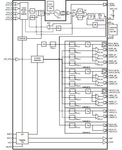
The 8V19N490B is a fully integrated FemtoClock® NG jitter attenuator and clock synthesizer designed as a high-performance clock solution for conditioning and frequency/phase management of wireless base station radio equipment boards. The device is optimized to deliver excellent phase noise performance as required in GSM, WCDMA, LTE, and LTE-A radio board implementations. The 8V19N490B supports JESD204B subclass 0 and 1 clocks.
A two-stage PLL architecture supports both jitter attenuation and frequency multiplication. The first stage PLL is the jitter attenuator and uses an external VCXO for best possible phase noise characteristics. The second stage PLL locks on the VCXO-PLL output signal and synthesizes the target frequency.
The device supports the clock generation of high-frequency clocks from the selected VCO and low-frequency synchronization signals (SYSREF). SYSREF signals are internally synchronized to the clock signals. Delay functions exist for achieving alignment and controlled phase delay between system reference and clock signals and to align/delay individual output signals. The four redundant inputs are monitored for activity. Four selectable clock switching modes are provided to handle clock input failure scenarios. Auto-lock, individually programmable output frequency dividers, and phase adjustment capabilities are added for flexibility. The device is configured through a 3-wire SPI interface and reports lock and signal loss status in internal registers and via a lock detect (LOCK) output. Internal status bit changes can also be reported via the nINT output. The 8V19N490B is ideal for driving converter circuits in wireless infrastructure, radar/imaging, and instrumentation/medical applications.
For information regarding evaluation boards and material, please contact your local sales representative.
The 8V19N490B evaluation board is designed to enable customers to evaluate the functionality and performance of the 1966.08MHz FemtoClock® NG Jitter Attenuator and...
点击产品选项表中的产品,查找 SamacSys 中的原理图符号、PCB 足迹和 3D CAD 模型。点击产品选项表中的产品,查找 SamacSys 中的原理图符号、PCB 足迹和 3D CAD 模型。

当前筛选条件