封装信息
| CAD 模型: | View CAD Model |
| Pkg. Type: | WAFER |
| Pkg. Code: | DICE |
| Lead Count (#): | |
| Pkg. Dimensions (mm): | 0.0 x 0.0 x 0.0 |
| Pitch (mm): |
环境和出口类别
| Moisture Sensitivity Level (MSL) | 1 |
| Pb (Lead) Free | Yes |
| ECCN (US) | EAR99 |
| HTS (US) | 8542.39.0090 |
产品属性
| Lead Count (#) | 0 |
| Carrier Type | Wafer |
| Moisture Sensitivity Level (MSL) | 1 |
| Output Freq Range (MHz) | 60 - 200 |
| Pkg. Dimensions (mm) | 0.0 x 0.0 x 0.0 |
| Qty. per Reel (#) | 0 |
| Qty. per Carrier (#) | 0 |
| Pb (Lead) Free | Yes |
| Pb Free Category | e3 Sn |
| Temp. Range (°C) | 0 to 70°C |
| Core Voltage (V) | 3.3 |
| Feedback Input | No |
| Input Freq (MHz) | 5 - 50 |
| Input Type | Crystal, LVCMOS |
| Inputs (#) | 1 |
| MOQ | 8000 |
| Output Banks (#) | 1 |
| Output Type | LVCMOS |
| Output Voltage (V) | 3.3 |
| Outputs (#) | 1 |
| Period Jitter Typ P-P (ps) | 70 |
| Pkg. Type | WAFER |
| Product Category | General Purpose Clocks |
| Prog. Clock | No |
| Reference Output | No |
| Requires Terms and Conditions | Does not require acceptance of Terms and Conditions |
| Spread Spectrum | No |
| Tape & Reel | No |
有关 501A 的资源
描述
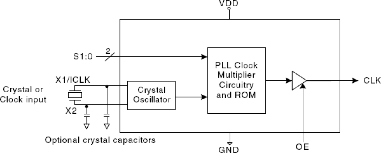
The 501A is the most cost effective way to generate a high quality, high frequency clock output from a lower frequency crystal or clock input. It is designed to replace crystal oscillators in most electronic systems. Using Phase-Locked Loop (PLL) techniques, the device uses a standard fundamental mode, inexpensive crystal to produce output clocks up to 200 MHz. Stored in the chip's ROM is the ability to generate nine different multiplication factors, allowing one chip to output many common frequencies (see table on page 2). The device also has an output enable pin which tri-states the clock output when the OE pin is taken low. This product is intended for clock generation. It has low output jitter (variation in the output period), but input to output skew and jitter are not defined or guaranteed. For applications which require defined input to output skew, use the 570B.
