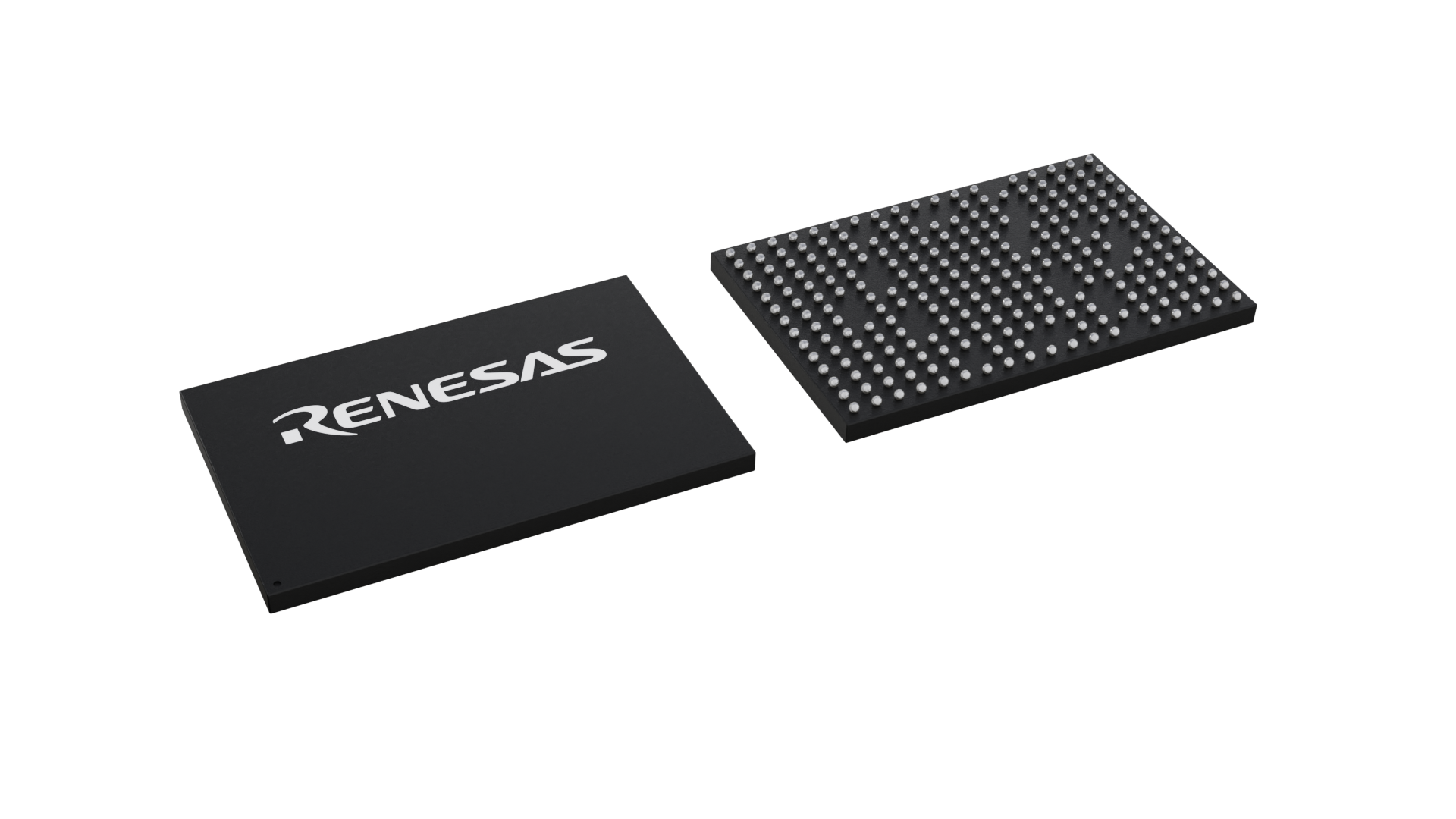
封装信息
| CAD 模型: | View CAD Model |
| Pkg. Type: | FCCSP |
| Pkg. Code: | AVG240 |
| Lead Count (#): | 240 |
| Pkg. Dimensions (mm): | 13.5 x 8.7 x 0.9 |
| Pitch (mm): | 0.65 |
环境和出口类别
| Moisture Sensitivity Level (MSL) | 3 |
| Pb (Lead) Free | Yes |
| ECCN (US) | EAR99 |
| HTS (US) | 8542.39.0090 |
| RoHS (5RCD0148HC3AVG8) | 英语日文 |
产品属性
| Lead Count (#) | 240 |
| Carrier Type | Reel |
| Moisture Sensitivity Level (MSL) | 3 |
| Qty. per Reel (#) | 3000 |
| Qty. per Carrier (#) | 0 |
| Pb (Lead) Free | Yes |
| Pb Free Category | e1 SnAgCu |
| Temp. Range (°C) | 0 to 125°C |
| Comm. Interface | I2C, I3C |
| Function | DDR5 Gen 1.0 Server RCD |
| Input Voltage Range (V) | 1.04 - 1.16 |
| Lead Compliant | No |
| Length (mm) | 13.5 |
| MOQ | 3000 |
| Pitch (mm) | 0.65 |
| Pkg. Dimensions (mm) | 13.5 x 8.7 x 0.9 |
| Pkg. Type | FCCSP |
| Reel Size (in) | 13 |
| Supply Voltage (V) | 1.04 - 1.16 |
| Tape & Reel | Yes |
| Thickness (mm) | 0.9 |
| Width (mm) | 8.7 |
| 已发布 | No |
有关 5RCD0148 的资源
描述
The 5RCD0148HC2 (RCD) is a registering clock driver used on DDR5 RDIMMs and LRDIMMs. It supports DDR5 server speeds up to 4800 MT/s. Its primary function is to buffer the Command Address (CA) bus, chip selects, and clock between the host controller and the DRAMs. It also creates a BCOM bus to control the data buffers for LRDIMMs.
The 5RCD0148HC2 contains two separate channels with some common logic such as clocking, but otherwise operate independently of each other. Each channel has a 7-bit double data rate CA bus input, a single parity input, two chip-select inputs, produces two copies of 14-bit single data rate CA bus outputs and two copies of the chip-select outputs. The RCD has a common clock input and PLL but produces separate clock outputs to the DRAM channels.
