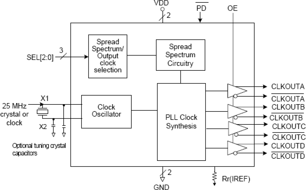
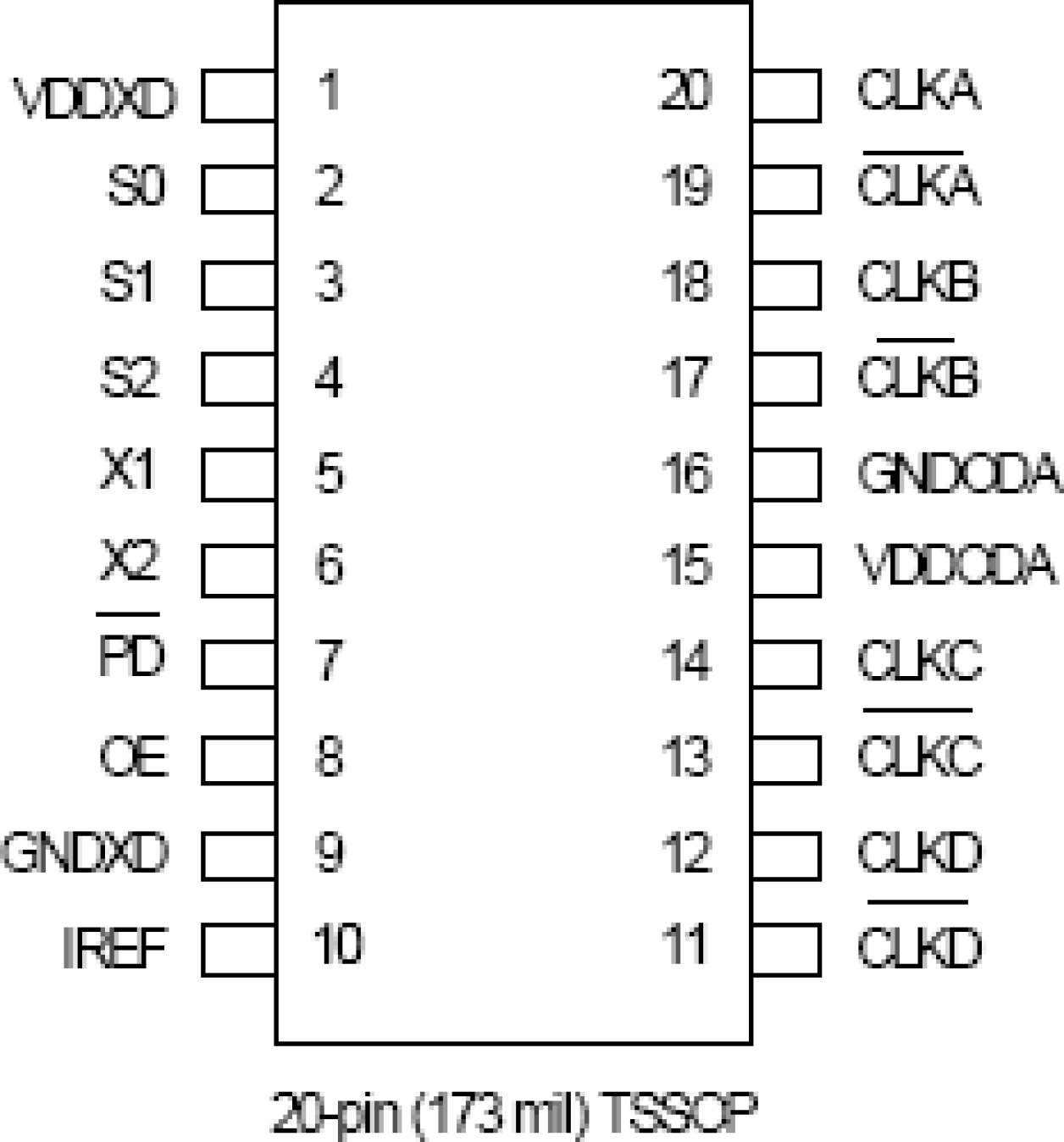
特性
- 4 - 0.7V current mode differential HCSL output pairs
- 20-pin TSSOP package
- small board footprint
- Spread-spectrum capable
- reduces EMI
- Outputs can be terminated to LVDS
- can drive a wider variety of devices
- Power down pin
- greater system power management
- OE control pin
- greater system power management
- Spread% and frequency pin selection
- no software required to configure device
- Industrial temperature range available
- supports demanding embedded applications
- For PCIe Gen3 applications, see the 5V41236
- Cycle-to-cycle jitter < 100 ps
- Output-to-output skew < 50 ps
- PCIe Gen2 phase jitter < 3.0ps RMS
描述
The 5V41066 is a PCIe Gen2 compliant spread-spectrum-capable clock generator. The device has 4 differential HCSL outputs and can be used in communication or embedded systems to substantially reduce electro-magnetic interference (EMI). The spread amount and output frequency are selectable via select pins.
产品参数
| 属性 | 值 |
|---|---|
| Diff. Outputs | 4 |
| Diff. Output Signaling | HCSL |
| Output Freq Range (MHz) | 100 - 100, 200 - 200 |
| Power Consumption Typ (mW) | 413 |
| Supply Voltage (V) | 3.3 - 3.3 |
| Output Type | HCSL |
| Xtal Freq (MHz) | 25 - 25 |
| Diff. Termination Resistors | 16 |
| Package Area (mm²) | 28.6 |
| Battery Backup | No |
| Battery Seal | No |
| CPU Supervisory Function POR | No |
| Crystal Frequency Trimming | No |
| Frequency Out Pin | No |
| Inputs (#) | 1 |
| Input Freq (MHz) | 25 - 25 |
| Input Type | Crystal, LVCMOS |
| Output Banks (#) | 1 |
| Core Voltage (V) | 3.3 |
| Output Voltage (V) | 3.3 |
封装选项
| Pkg. Type | Pkg. Dimensions (mm) | Lead Count (#) | Pitch (mm) |
|---|---|---|---|
| TSSOP | 6.5 x 4.4 x 1.0 | 20 | 0.65 |
当前筛选条件
筛选
软件与工具
样例程序
模拟模型
This is the first video in our PCIe series. In this video, we define PCIe architectures, focusing on common and separate clock architectures. Watch the rest of the video series below where Ron will cover the impact of different timing architectures.
In this episode, Ron Wade from IDT (acquired by Renesas) explains PCIe common clocking and its impact on timing solutions. Learn about using a single clock source, fan-out buffers, and the considerations for spread spectrum and non-spread spectrum clocking in PCIe systems.
In this video, we explore PCIe with separate reference clocks and the effects of clock selection. Learn how separate reference clocks work and their impact on system performance and stability.
This video provides a high-level overview of Separate Reference Clock with Independent Spread (SRIS) architectures for PCI Express systems, additional performance requirements that this clocking architecture imposes on the reference clocks, and some system implications encountered trying to implement the architecture.


