特性
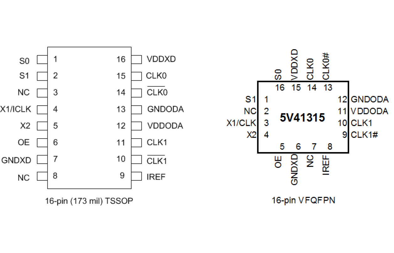
- 16-pin TSSOP or VFQFPN package; small board footprint
- Outputs can be terminated to LVDS; can drive a wider variety of devices
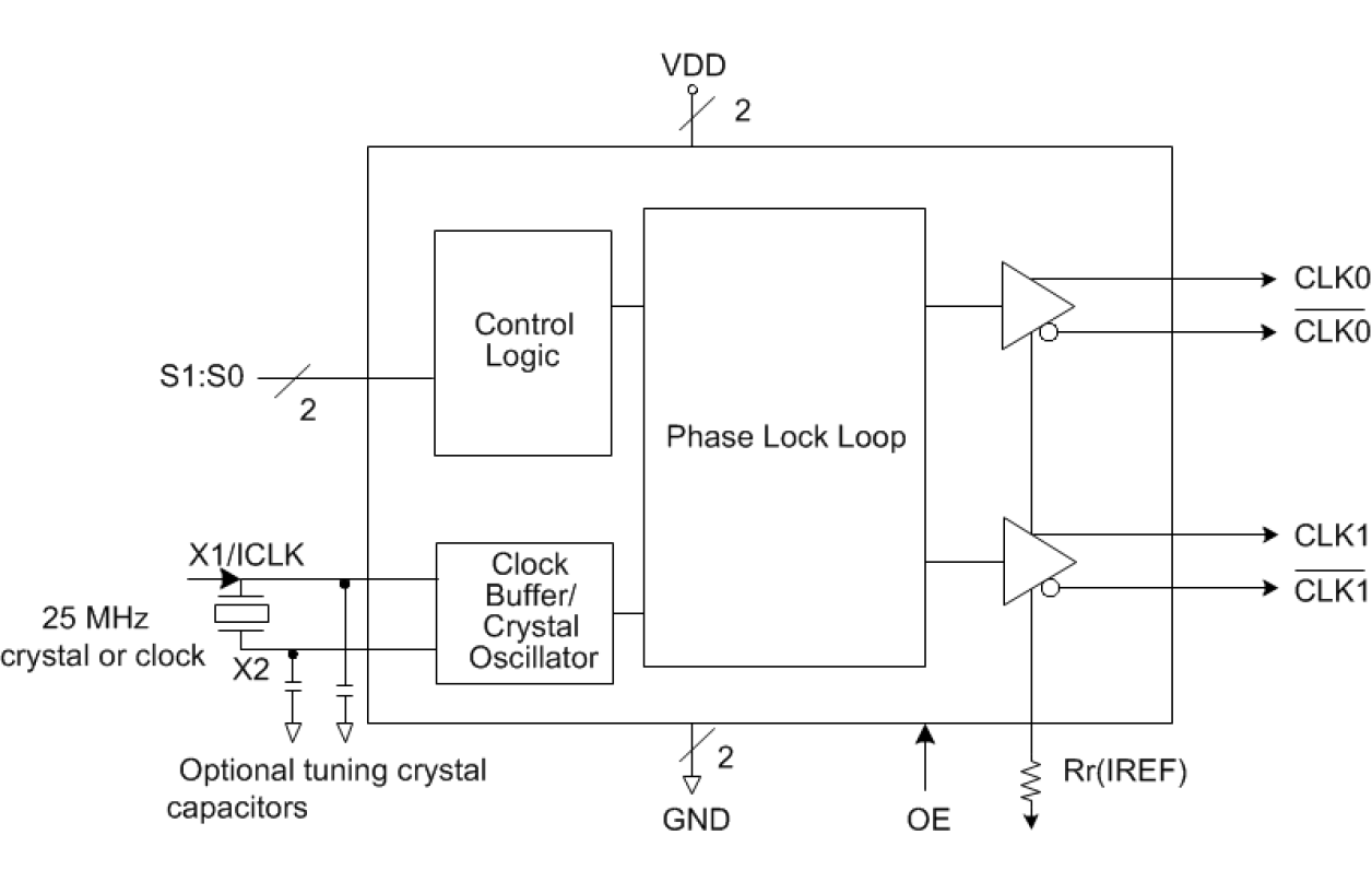
- OE control pin; greater system power management
- Industrial temperature range available; supports demanding embedded applications
- Cycle-to-cycle jitter: 80ps
- Output-to-output skew: <50 ps
- PCIe Gen2 phase jitter: <3.0ps RMS (Common Clock)
- PCIe Gen3 phase jitter: <1.0ps RMS (Common Clock)
- Low Phase Noise: 12KHz to 20MHz <6ps RMS
描述
The IDT5V41315 is a PCIe Gen1/2/3 clock synthesizer suitable for use in both Common-Clocked and Separate Reference clock with No Spread (SRNS) timing architectures. The IDT5V41315 uses a 25MHz input to generate 4 different output frequencies. The output frequency is selectable via select pins.
当前筛选条件
筛选
软件与工具
样例程序
模拟模型
This is the first video in our PCIe series. In this video, we define PCIe architectures, focusing on common and separate clock architectures. Watch the rest of the video series below where Ron will cover the impact of different timing architectures.
In this episode, Ron Wade from IDT (acquired by Renesas) explains PCIe common clocking and its impact on timing solutions. Learn about using a single clock source, fan-out buffers, and the considerations for spread spectrum and non-spread spectrum clocking in PCIe systems.
In this video, we explore PCIe with separate reference clocks and the effects of clock selection. Learn how separate reference clocks work and their impact on system performance and stability.
This video provides a high-level overview of Separate Reference Clock with Independent Spread (SRIS) architectures for PCI Express systems, additional performance requirements that this clocking architecture imposes on the reference clocks, and some system implications encountered trying to implement the architecture.