封装信息
| Pkg. Type: | TQFP |
| Pkg. Code: | PRG32 |
| Lead Count (#): | 32 |
| Pkg. Dimensions (mm): | 7.0 x 7.0 x 1.4 |
| Pitch (mm): | 0.8 |
环境和出口类别
| Pb (Lead) Free | Yes |
| ECCN (US) | EAR99 |
| HTS (US) | 8542.39.0090 |
| Moisture Sensitivity Level (MSL) | 3 |
产品属性
| Pkg. Type | TQFP |
| Lead Count (#) | 32 |
| Pb (Lead) Free | Yes |
| Carrier Type | Tray |
| Core Voltage (V) | 3.3V, 2.5V |
| Divider Value | 2, 4, 8 |
| Input Freq (MHz) | 25 - 200 |
| Input Type | LVTTL, LVPECL |
| Inputs (#) | 2 |
| Length (mm) | 7 |
| MOQ | 125 |
| Moisture Sensitivity Level (MSL) | 3 |
| Output Banks (#) | 4 |
| Output Freq Range (MHz) | 25 - 200 |
| Output Signaling | LVCMOS, LVTTL |
| Output Skew (ps) | 150 |
| Output Type | LVCMOS, LVTTL |
| Output Voltage (V) | 3.3V, 2.5V |
| Outputs (#) | 9 |
| Package Area (mm²) | 49 |
| Pb Free Category | e3 Sn |
| Pitch (mm) | 0.8 |
| Pkg. Dimensions (mm) | 7.0 x 7.0 x 1.4 |
| Qty. per Carrier (#) | 250 |
| Qty. per Reel (#) | 0 |
| Requires Terms and Conditions | Does not require acceptance of Terms and Conditions |
| Tape & Reel | No |
| Temp. Range (°C) | -40 to 85°C |
| Thickness (mm) | 1.4 |
| VCO Max Freq (MHz) | 400 |
| VCO Min Freq (MHz) | 200 |
| Width (mm) | 7 |
| 已发布 | No |
有关 5V9351 的资源
描述
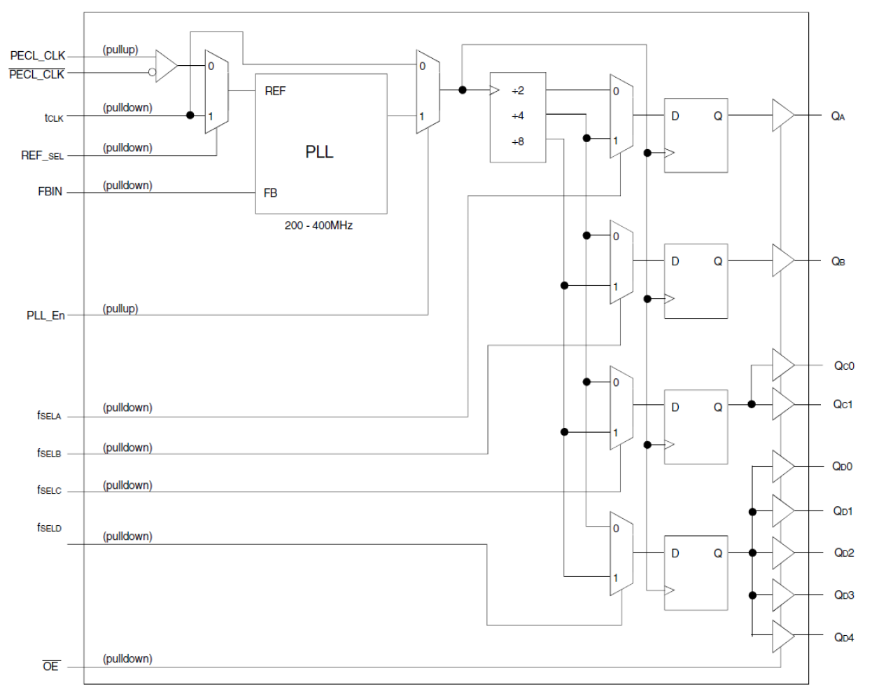
The 5V9351 is a high performance, zero delay, low skew, phase-lock loop (PLL) clock driver. It has four banks of configurable outputs. The 5V9351 uses a differential PECL reference input and an external feedback input. These features allow the 5V9351 to be used as a zero delay, low skew fan-out buffer. REF_SEL allows selection between PECL input or TCLK, a CMOS clock driver input. If PLL_EN is set to low and REF_SEL to high, it will bypass the PLL. By doing so, the 5V9351 will be in clock buffer mode. Any clock applied to TCLK will be divided down to four output banks. When PLL_EN is set high, PLL is enabled. Any clock applied to TCLK will be clocked in both phase and frequency to FBIN. PECL clock is activated by setting REF_SEL to low.

