特性
- Eight zero delay outputs
- <250ps of output to output skew
- Selectable positive or negative edge synchronization
- Synchronous output enable
- Output frequency: 15MHz to 85MHz
- 3 skew grades:
- IDT5V9910A-2: tSKEW0<250ps
- IDT5V9910A-5: tSKEW0<500ps
- IDT5V9910A-7: tSKEW0<750ps
- 3-level inputs for PLL range control
- PLL bypass for DC testing
- External feedback, internal loop filter
- 12mA balanced drive outputs
- Low Jitter: <200ps peak-to-peak
- Available in SOIC package
- Functional replacement part: 8T49N008-dddNLGI
描述
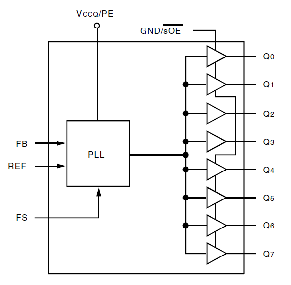
The 5V9910A is a high fanout phase locked-loop clock driver intended for high performance computing and data-communications applications. It has eight zero delay LVTTL outputs. When the GND/sOE pin is held low, all the outputs are synchronously enabled. However, if GND/sOE is held high, all the outputs except Q2 and Q3 are synchronously disabled. Furthermore, when the VCCQ/PE is held high, all the outputs are synchronized with the positive edge of the REF clock input. When VCCQ/ PE is held low, all the outputs are synchronized with the negative edge of REF. The FB signal is compared with the input REF signal at the phase detector in order to drive the VCO. Phase differences cause the VCO of the PLL to adjust upwards or downwards accordingly. An internal loop filter moderates the response of the VCO to the phase detector. The loop filter transfer function has been chosen to provide minimal jitter (or frequency variation) while still providing accurate responses to input frequency changes.
当前筛选条件

