封装信息
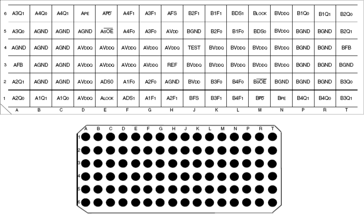
| Pkg. Type: | CABGA |
| Pkg. Code: | BFG96 |
| Lead Count (#): | 96 |
| Pkg. Dimensions (mm): | 13.5 x 5.5 x 1.4 |
| Pitch (mm): | 0.8 |
环境和出口类别
| Pb (Lead) Free | Yes |
| ECCN (US) | EAR99 |
| HTS (US) | 8542.39.0090 |
| Moisture Sensitivity Level (MSL) | 3 |
产品属性
| Pkg. Type | CABGA |
| Lead Count (#) | 96 |
| Pb (Lead) Free | Yes |
| Carrier Type | Tray |
| Advanced Features | Feedback Input |
| C-C Jitter Max P-P (ps) | 125 |
| Core Voltage (V) | 3.3 |
| Feedback Input | Yes |
| Input Freq (MHz) | 2 - 200 |
| Input Type | LVCMOS |
| Inputs (#) | 1 |
| Length (mm) | 13.5 |
| MOQ | 135 |
| Moisture Sensitivity Level (MSL) | 3 |
| Output Banks (#) | 8 |
| Output Freq Range (MHz) | 6 - 200 |
| Output Skew (ps) | 250 |
| Output Type | LVCMOS |
| Output Voltage (V) | 3.3 |
| Outputs (#) | 16 |
| Package Area (mm²) | 74.3 |
| Pb Free Category | e1 SnAgCu |
| Pitch (mm) | 0.8 |
| Pkg. Dimensions (mm) | 13.5 x 5.5 x 1.4 |
| Prog. Clock | No |
| Qty. per Carrier (#) | 270 |
| Qty. per Reel (#) | 0 |
| Requires Terms and Conditions | Does not require acceptance of Terms and Conditions |
| Tape & Reel | No |
| Temp. Range (°C) | -40 to 85°C |
| Thickness (mm) | 1.4 |
| Width (mm) | 5.5 |
| 已发布 | No |
有关 5V9955 的资源
描述
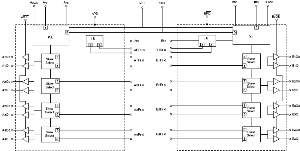
The IDT5V9955 is a high fanout 3.3V PLL based clock driver intended for high performance computing and data-communications applications. A key feature of the programmable skew is the ability of outputs to lead or lag the REF input signal. The IDT5V9955 has sixteen programmable skew outputs in eight banks of 2. The two separate PLLs allow the user to independently control A and B banks. Skew is controlled by 3-level input signals that may be hard-wired to appropriate HIGH-MID-LOW levels. The feedback input allows divide-by-functionality from 1 to 12 through the use of the xDS[1:0] inputs. This provides the user with frequency multiplication from 1 to 12 without using divided outputs for feedback. When the xsOE pin is held low, all the xbank outputs are synchronously enabled. However, if xsOE is held high, all the xbank outputs except x2Q0 and x2Q1 are synchronously disabled. The xLOCK is high when the xbank PLL has achieved phase lock. Furthermore, when xPE is held high, all the outputs are synchronized with the positive edge of the REF clock input. When xPE is held low, all the xbank outputs are synchronized with the negative edge of REF. The IDT5V9955 has LVTTL outputs with 12mA balanced drive outputs.


