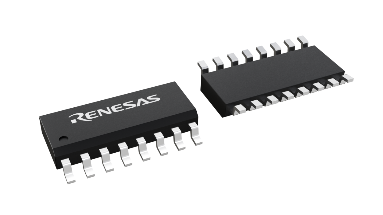
封装信息
| CAD 模型: | View CAD Model |
| Pkg. Type: | SOIC |
| Pkg. Code: | DCG16 |
| Lead Count (#): | 16 |
| Pkg. Dimensions (mm): | 9.9 x 3.9 x 1.5 |
| Pitch (mm): | 1.27 |
环境和出口类别
| Moisture Sensitivity Level (MSL) | 3 |
| Pb (Lead) Free | Yes |
| ECCN (US) | EAR99 |
| HTS (US) | 8542.39.0090 |
产品属性
| Lead Count (#) | 16 |
| Carrier Type | Tube |
| Moisture Sensitivity Level (MSL) | 3 |
| Qty. per Reel (#) | 0 |
| Qty. per Carrier (#) | 48 |
| Pb (Lead) Free | Yes |
| Pb Free Category | e3 Sn |
| Temp. Range (°C) | 0 to 70°C |
| Advanced Features | Feedback Input |
| Core Voltage (V) | 3.3V, 5V |
| Feedback Input | Yes |
| Input Freq (MHz) | 0.001 - 8 |
| Input Type | LVCMOS |
| Inputs (#) | 1 |
| Length (mm) | 9.9 |
| MOQ | 192 |
| Output Banks (#) | 2 |
| Output Freq Range (MHz) | 0.25 - 120 |
| Output Type | LVCMOS |
| Output Voltage (V) | 3.3V, 5V |
| Outputs (#) | 2 |
| Package Area (mm²) | 38.6 |
| Period Jitter Max P-P (ps) | 250 |
| Period Jitter Typ P-P (ps) | 150 |
| Pitch (mm) | 1.27 |
| Pkg. Dimensions (mm) | 9.9 x 3.9 x 1.5 |
| Pkg. Type | SOIC |
| Product Category | General Purpose Clocks |
| Prog. Clock | No |
| Reference Output | No |
| Requires Terms and Conditions | Does not require acceptance of Terms and Conditions |
| Spread Spectrum | No |
| Tape & Reel | No |
| Thickness (mm) | 1.5 |
| Width (mm) | 3.9 |
有关 673-01 的资源
描述
The 673-01 is a low cost, high performance Phase Locked Loop (PLL) designed for clock synthesis and synchronization. Included on the chip are the phase detector, charge pump, Voltage Controlled Oscillator (VCO), and two output buffers. One output buffer is a divide by two of the other. Through the use of external reference and VCO dividers (the 674-01), the user can customize the clock to lock to a wide variety of input frequencies. The 673-01 also has an output enable function that puts both outputs into a high-impedance state. The chip also has a power down feature which turns off the entire device. For applications that require low jitter or jitter attenuation, see the MK2069. For a smaller package, see the 663.


