特性
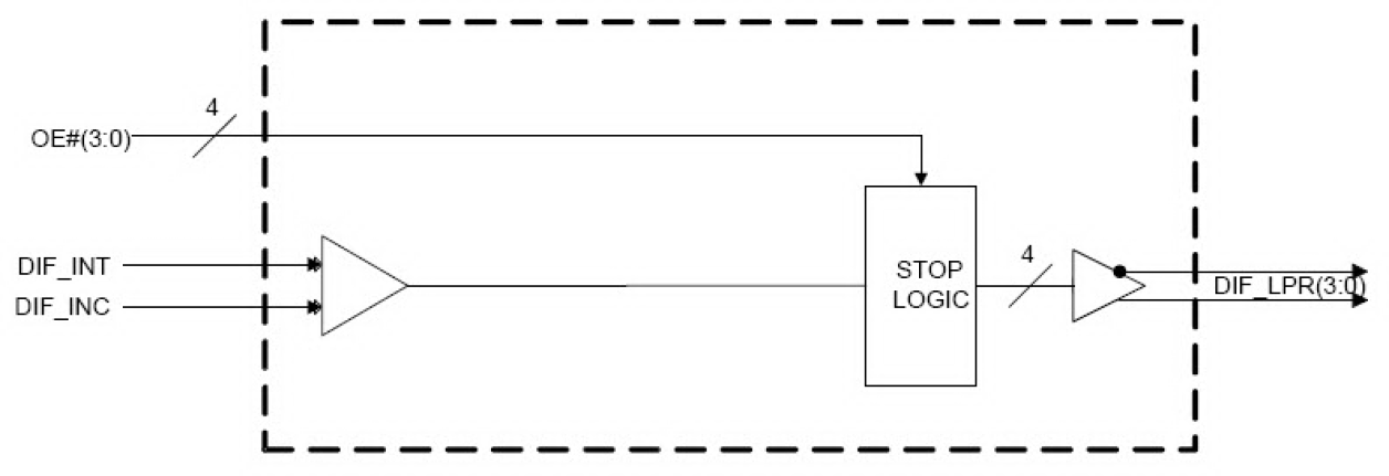
- 4 - low power differential output pairs
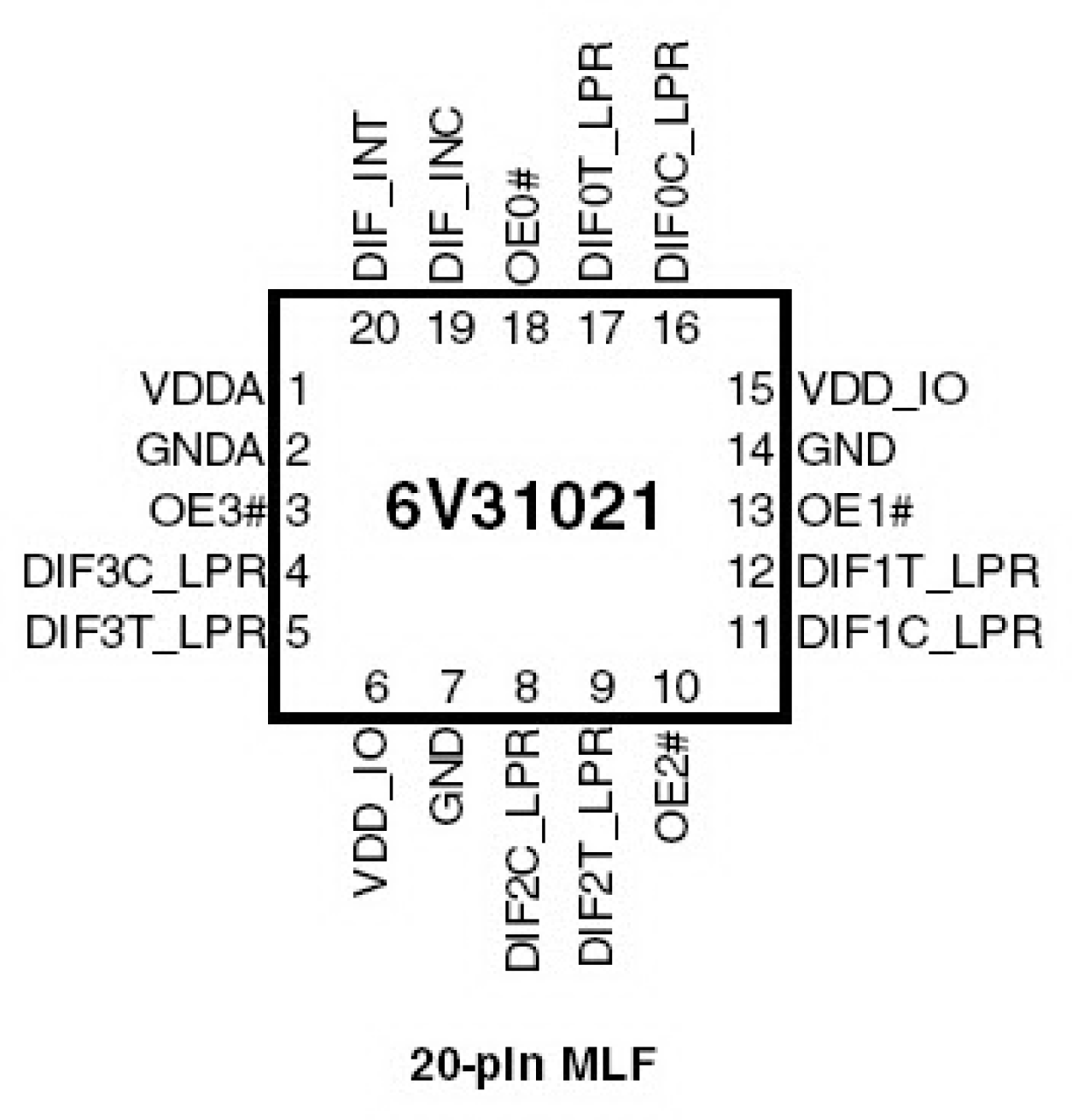
- Individual OE# control of each output pair
- Low power differential outputs
- Power down mode when all OE# are high
- Industrial temperature range
- 20-pin MLF
- Output cycle-cycle jitter <15 ps additive
- Output to Output skew: <50 ps
- PCIe Gen3 additive phase jitter <0.3 ps rms
- 10.3125G / 64 additive phase jitter <100 fs rms
描述
The IDT6V31021 is a 4-output low- power differential buffer. Each output has its own OE# pin. It has a maximum operating frequency of 167 MHz and supports all SERDES clock frequencies for Freescale QorIQ CPUs.
当前筛选条件


