特性
- Twenty LVCMOS/LVTTL outputs, 7? typical output impedance
- One LVCMOS/LVTTL clock input
- Maximum output frequency: 250MHz
- Selectable inverting and non-inverting outputs
- Bank enable logic allows unused banks to be disabled in reduced fanout applications
- Output skew: 300ps (maximum)
- Part-to-part skew: 700ps (maximum)
- Bank skew: 250ps (maximum)
- Multiple frequency skew: 350ps (maximum)
- 3.3V or mixed 3.3V input, 2.5V output operating supply
- 0°C to 70°C ambient operating temperature
描述
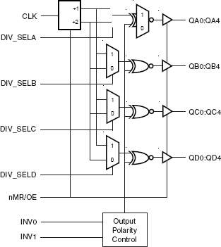
The 8701-01 is a low skew, ÷1, ÷2 LVCMOS/ LVTTL Clock Generator. The low impedance LVCMOS outputs are designed to drive 50? series or parallel terminated transmission lines. The effective fanout can be increased from 20 to 40 by utilizing the ability of the outputs to drive two series terminated lines. The divide select inputs, DIV_SELx, control the output frequency of each bank. The outputs can be utilized in the ÷1, ÷2 or a combination of ÷1 and ÷2 modes. The master reset/output enable input, nMR/OE, resets the internal dividers and controls the active and high impedance states of all outputs. The output polarity inputs, INV0:1, control the polarity (inverting or non-inverting) of the outputs of each bank. Outputs QA0:QA4 are inverting for every combination of the INV0:1 input. The timing relationship between the inverting and non-inverting outputs at different frequencies is shown in the Timing Diagrams. The 8701-01 is characterized at 3.3V and mixed 3.3V input supply, and 2.5V output supply operating modes. Guaranteed bank, output and part-to-part skew characteristics make the 8701-01 ideal for those clock distribution applications demanding well defined performance and repeatability.