特性
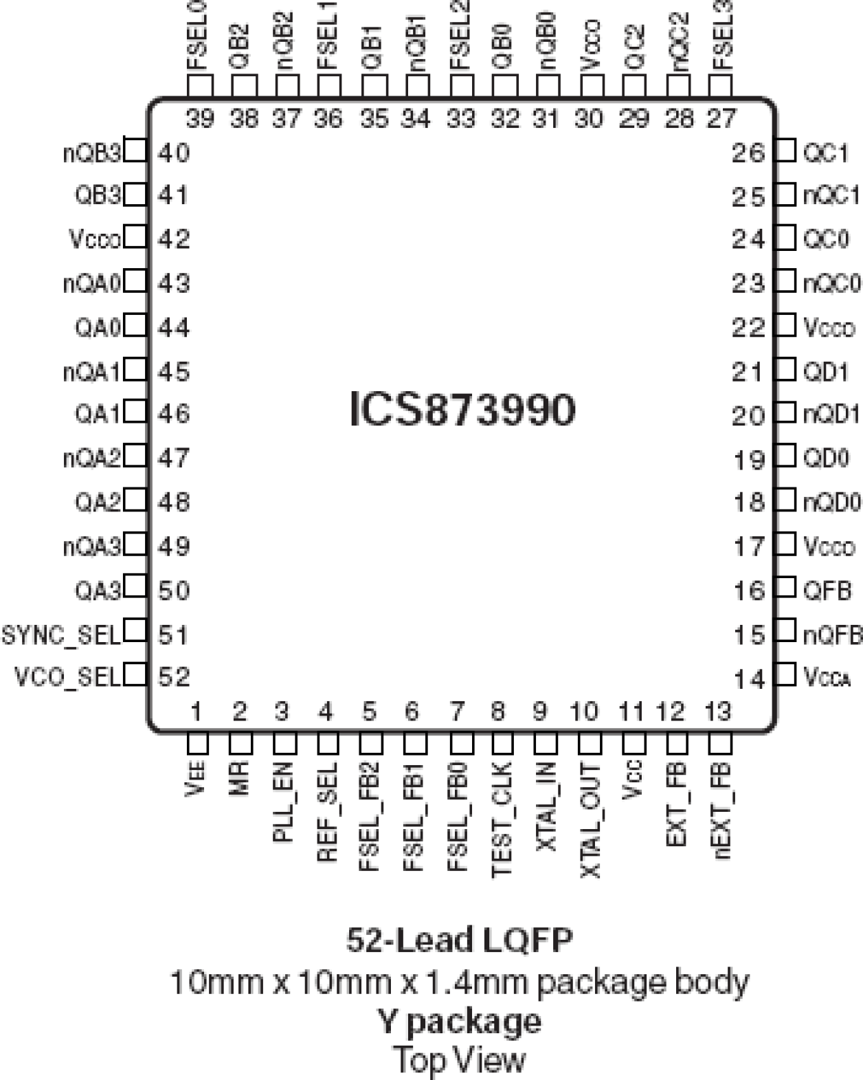
- 14 differential LVPECL outputs
- Selectable crystal oscillator interface or TEST_CLK inputs
- TEST_CLK accepts the following input levels: LVCMOS, LVTTL
- Output frequency: 400MHz (maximum)
- Crystal input frequency range: 10MHz to 25MHz
- VCO range: 200MHz to 800MHz
- Output skew: 250ps (maximum)
- Cycle-to-cycle jitter: ±50ps (typical)
- LVPECL mode operating voltage supply range: VCC = 3.135V to 3.465V, VEE = 0V
- ECL mode operating voltage supply range: VCC = 0V, VEE = -3.465V to -3.135V
- 0°C to 70°C ambient operating temperature
- Industrial temperature available upon request
- Lead-Free package fully RoHS compliant
描述
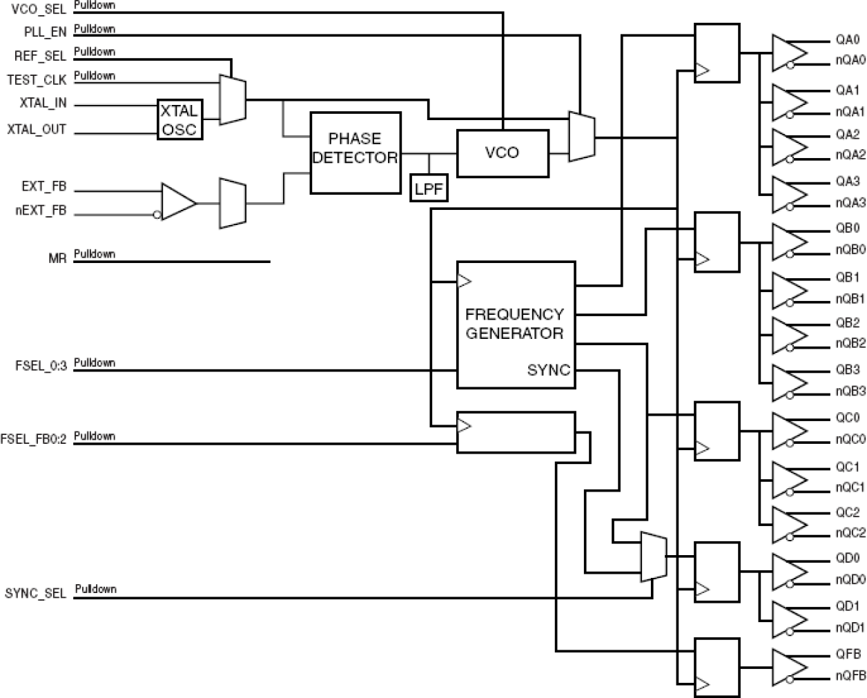
The 873990 is a low voltage, low skew, 3.3V LVPECL/ ECL Clock Generator. The 873990 has two selectable clock inputs. The XTAL1 and XTAL2 are used to interface to a crystal and the TEST_CLK pin can accept a LVCMOS or LVTTL input. This device has a fully integrated PLL along with frequency configurable outputs. An external feedback input and output regenerates clocks with "zero delay". The four independent banks of outputs each have their own output dividers, which allow the device to generate a multitude of different bank frequency ratios and output-to-input frequency ratios. The output frequency range is 25MHz to 400MHz and the input frequency range is 6.25MHz to 125MHz. The PLL_SEL input can be used to bypass the PLL for test and system debug purposes. In bypass mode, the input clock is routed around the PLL and into the internal output dividers. The 873990 also has a SYNC output which can be used for system synchronization purposes. It monitors Bank A and Bank C outputs for coincident rising edges and signals a pulse per the timing diagrams in this data sheet. This feature is used primarily in applications where Bank A and Bank C are running at different frequencies, and is particularly useful when they are running at non-integer multiples of each other.
当前筛选条件


