特性
- Fully integrated PLL
- Six LVCMOS/LVTTL outputs, 7? typical output impedance
- Selectable differential CLK0, nCLK0 or LVCMOS/LVTTL clock for redundant clock applications
- Maximum output frequency: 240MHz
- VCO range: 220MHz to 480MHz
- External feedback for "zero delay" clock regeneration
- Output skew: 165ps (maximum)
- Cycle-to-cycle jitter: 45ps (maximum)
- 3.3V supply voltage
- -40°C to 85°C ambient operating temperature
- Contact IDT for replacement device at [email protected]
描述
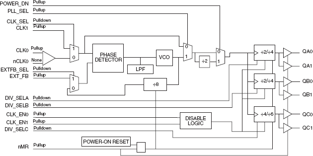
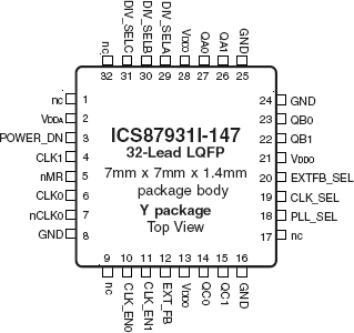
The 87931I-147 is a low voltage, low skew LVCMOS/LVTTL Clock Multiplier/Zero Delay Buffer. With output frequencies up to 240MHz, the 87931I is targeted for high performance clock applications. Along with a fully integrated PLL, the 87931I-147 contains frequency configurable outputs and an external feedback input for regenerating clocks with "zero delay". Selectable clock inputs, CLK1 and differential CLK0, nCLK0 support redundant clock applications. The CLK_SEL input determines which reference clock is used. The output divider values of Bank A, B and C are controlled by the DIV_SELA, DIV_SELB and DIV_SELC, respectively. For test and system debug purposes, the PLL_SEL input allows the PLL to be bypassed. When LOW, the nMR input resets the internal dividers and forces the outputs to the high impedance state. The effective fanout of the 87931I-147 can be increased to 12 by utilizing the ability of each output to drive two series terminated transmission lines.
当前筛选条件


