封装信息
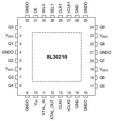
| Lead Count (#) | 32 |
| Pkg. Code | NLG32 |
| Pitch (mm) | 0.5 |
| Pkg. Type | VFQFPN |
| Pkg. Dimensions (mm) | 5.0 x 5.0 x 0.9 |
环境和出口类别
| Moisture Sensitivity Level (MSL) | 3 |
| Pb (Lead) Free | Yes |
| ECCN (US) | NLR |
| HTS (US) | 8542390001 |
产品属性
| Lead Count (#) | 32 |
| Carrier Type | Tray |
| Moisture Sensitivity Level (MSL) | 3 |
| Qty. per Reel (#) | 0 |
| Qty. per Carrier (#) | 490 |
| Pb (Lead) Free | Yes |
| Pb Free Category | e3 Sn |
| Temp. Range | -40 to +85°C |
| Country of Assembly | Taiwan |
| Country of Wafer Fabrication | Singapore |
| Price (USD) | 1ku | 2.22171 |
| Additive Phase Jitter Typ RMS (fs) | 30 |
| Additive Phase Jitter Typ RMS (ps) | 0.03 |
| Core Voltage (V) | 2.5, 3.3 |
| Family Name | 8L30 |
| Function | Buffer, Multiplexer |
| Input Freq (MHz) | 0 - 200 |
| Input Type | LVCMOS, LVPECL, LVDS, HCSL, Crystal |
| Inputs (#) | 3 |
| Length (mm) | 5 |
| MOQ | 490 |
| Output Banks (#) | 2 |
| Output Freq Range (MHz) | 0 - 200 |
| Output Skew (ps) | 30 |
| Output Type | LVCMOS |
| Output Voltage (V) | 3.3, 2.5, 1.8, 1.5 |
| Outputs (#) | 10 |
| Package Area (mm²) | 25.0 |
| Pitch (mm) | 0.5 |
| Pkg. Dimensions (mm) | 5.0 x 5.0 x 0.9 |
| Pkg. Type | VFQFPN |
| Requires Terms and Conditions | Does not require acceptance of Terms and Conditions |
| Tape & Reel | No |
| Thickness (mm) | 0.9 |
| Width (mm) | 5 |
有关 8L30210 的资源
描述
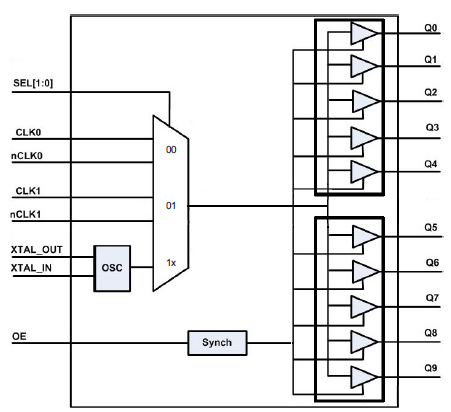
The 8L30210 is a low skew, 1-to-10 LVCMOS/LVTTL fanout buffer. The low impedance LVCMOS/LVTTL outputs are designed to drive 50Ω series or parallel terminated transmission lines.
The 8L30210 is characterized at full 3.3V and 2.5V, mixed 3.3V/2.5V, 3.3V/1.8V, 3.3V/1.5V, 2.5V/1.8V, and 2.5V/1.5V output operating supply modes. The input clock is selected from two differential clock inputs or a crystal input. The differential input can be wired to accept a single-ended input. The internal oscillator circuit is automatically disabled if the crystal input is not selected.

